A High Density Integrated Optical Waveguide

An integrated optical waveguide, high-density technology, applied in the field of integrated photonics, can solve the problems of waveguide spacing, wavelength sensitivity and dependence, etc., and achieve the effects of easy mass production, saving processing costs, and good robustness

Active Publication Date: 2021-06-08
NANJING UNIV
View PDF5 Cites 0 Cited by
  • Summary
  • Abstract
  • Description
  • Claims
  • Application Information

AI Technical Summary

Problems solved by technology

[0005] The purpose of the present invention is to provide a high-density integrated optical waveguide to solve the problem that the current integrated chips based on straight waveguides cannot get rid of the sensitivity and dependence on parameters such as waveguide spacing and wavelength under high-density integration

Method used


Image

  • A High Density Integrated Optical Waveguide
  • A High Density Integrated Optical Waveguide
  • A High Density Integrated Optical Waveguide

Examples


Embodiment Construction

[0054] The following will clearly and completely describe the technical solutions in the embodiments of the present invention with reference to the accompanying drawings in the embodiments of the present invention. Obviously, the described embodiments are only some, not all, embodiments of the present invention. Based on the embodiments of the present invention, all other embodiments obtained by persons of ordinary skill in the art without making creative efforts belong to the protection scope of the present invention.

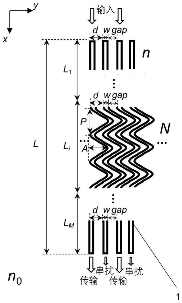
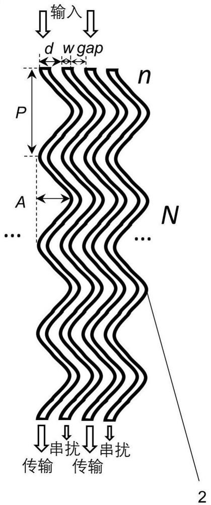
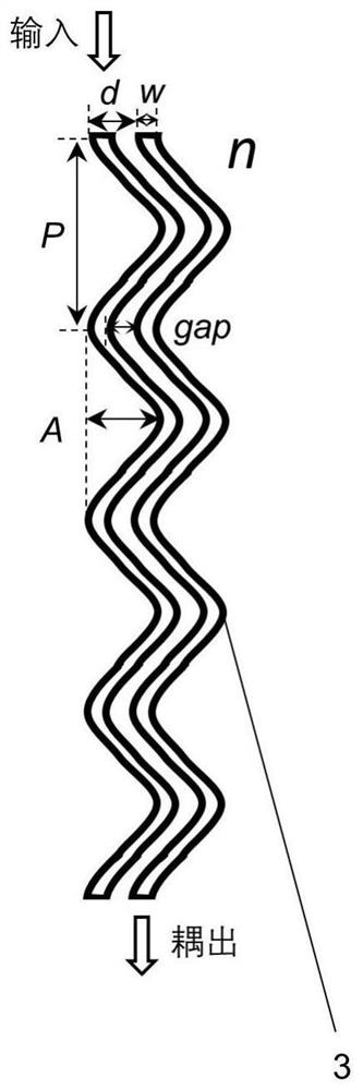
[0055] The purpose of the present invention is to provide a high-density integrated optical waveguide, which uses the positive and negative coupling cascade brought by straight waveguide and curved waveguide cascade to realize broadband low crosstalk optical waveguide transmission; adopts the zero coupling brought by curved waveguide for the stability of wavelength To achieve broadband low-crosstalk optical waveguide transmission; using the negative coupling br...


PUM


Abstract

The invention relates to a high-density integrated optical waveguide. The optical waveguide is arranged on a waveguide substrate, including: a plurality of curved waveguides; a rectangular coordinate system is established with the bending direction of the curved waveguides as the y-axis and the light propagation direction as the x-axis; and based on the rectangular coordinate system , the curved waveguide is periodically bent in the curved direction along the propagation direction; a plurality of curved waveguides are arranged in parallel along the y-axis direction, and the curved waveguides are perpendicular to the y-axis direction, forming A curved waveguide array; realizing the optical waveguide signal transmission function or the optical waveguide directional coupling function of the optical waveguide by adjusting the coupling coefficient between the curved waveguides. The optical waveguide provided by the invention gets rid of the sensitivity and dependence on parameters such as waveguide spacing and wavelength under high-density integration, so it has structural robustness and broadband characteristics.

Description

technical field [0001] The invention relates to the field of integrated photons, in particular to a high-density integrated optical waveguide. Background technique [0002] With the rise of the modern Internet of Things, big data and other industries, human society's demand for information processing such as higher speed, larger broadband network capacity, and stronger confidentiality has increased sharply, and electrical chips have obviously reached the bottleneck stage. In the same way as the development of integrated circuits, integrating two or more discrete optical components on a small substrate (below the centimeter level) can form an integrated optical chip system that realizes a certain function. It has high speed, low power consumption and Due to the advantages of high-density integration, it is expected to become a promising development direction for high-capacity, high-speed information systems. [0003] Silicon-on-insulator (SOI) has become one of the most wide...

Claims


Application Information

Patent Timeline
Patent Type & Authority Patents(China)
IPC IPC(8): G02B6/125G02B6/122
CPCG02B6/125G02B6/122G02B2006/12119
Inventor 李涛宋万鸽祝世宁
Owner NANJING UNIV
Why Eureka
Try Eureka