Ga2O3 film and preparation method thereof

A ga2o3 thin film technology, applied in the field of Ga2O3 thin film and its preparation, can solve the problems of long response time, low comprehensive performance of ultraviolet detectors, less research work, etc., and achieve the effect of short response time

Active Publication Date: 2020-09-25
CHANGCHUN INST OF OPTICS FINE MECHANICS & PHYSICS CHINESE ACAD OF SCI
View PDF2 Cites 2 Cited by
  • Summary
  • Abstract
  • Description
  • Claims
  • Application Information

AI Technical Summary

Problems solved by technology

But since the current Ga 2 o 3 The overall performance of the UV detector of the material is still relatively low, especially the response time of the device with higher responsivity is often longer
Practice has shown that a very small amount of impurities can change its performance, but there is little related research work at present, and how to use a suitable doping method to greatly improve the overall performance of the device remains to be studied

Method used


Image

  • Ga2O3 film and preparation method thereof
  • Ga2O3 film and preparation method thereof
  • Ga2O3 film and preparation method thereof

Examples


preparation example Construction

[0024] This application provides a Ga 2 o 3 The preparation method of the thin film by the chemical vapor deposition method in the metal organic compound on the Ga 2 o 3 The thin film is doped with a trace amount of magnesium, so that the thin film has high ultraviolet responsivity and short response time when applied to ultraviolet detectors. Specifically, the embodiment of the present invention discloses a Ga 2 o 3 The preparation method of thin film, comprises the following steps:

[0025] Using organic gallium compounds as the gallium source and high-purity oxygen as the oxygen source, metal-organic chemical vapor deposition is used to deposit on the surface of the substrate, and Ga is obtained after cooling down. 2 o 3 film;

[0026] in Ga 2 o 3 In the process of film growth, the organomagnesium compound is supplemented intermittently, and the time for supplementing the organomagnesium compound begins at Ga 2 o 3 0.1 to 6 hours after the film starts to grow, it...

Embodiment 1

[0039] Put the cleaned sapphire substrate into the MOCVD growth chamber, turn on the molecular pump, and make the vacuum degree of the backside of the chamber reach within 100Pa; raise the substrate temperature to 1100°C, and after pretreatment for 0.5h, lower the temperature to growth The temperature is 800°C; nitrogen gas is introduced to make the vacuum degree of the chamber during the growth process 2×10 3 Pa;

[0040] Using trimethylgallium as the gallium source, the carrier gas flow rate of the gallium source is 25sccm, and the flow rate of the oxygen gas is 250sccm; during the growth process, dimethylmagnesocene is used as the magnesium source, and the magnesium source is turned on after 0.2h of growth, and the magnesium The carrier gas flow rate of the source is 4sccm, open the magnesium source for 30s, close for 120s, repeat twenty times, then stop adding the magnesium source;

[0041] The entire growth process lasted 2 hours (including the time of turning on the mag...

Embodiment 2

[0053] In order to verify the influence of the starting time of the magnesium source on the properties of the film, other conditions were the same as in Example 1 except that the starting time of the magnesium source was changed. The start-up times of samples numbered 2-1, 2-2, 2-3, and 2-4 are respectively 0.1h, 0.5h, 0.8h, and 1h (in Example 1, the magnesium source is turned on after starting growth for 0.2h);

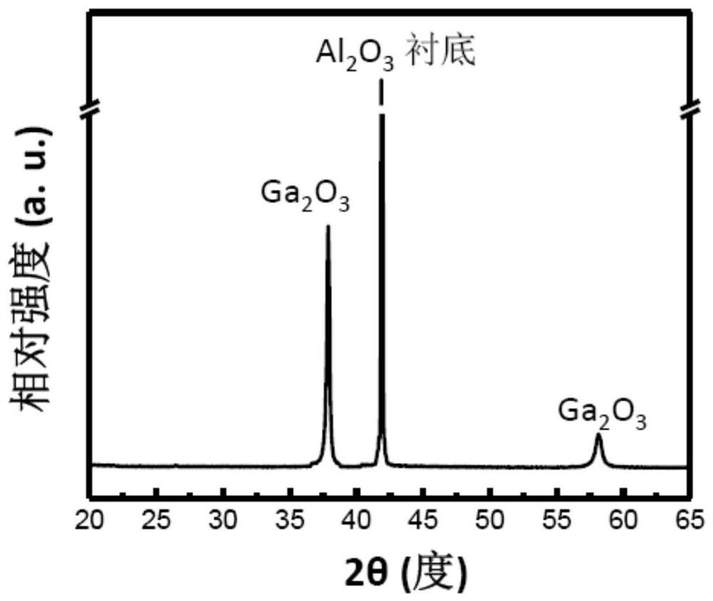
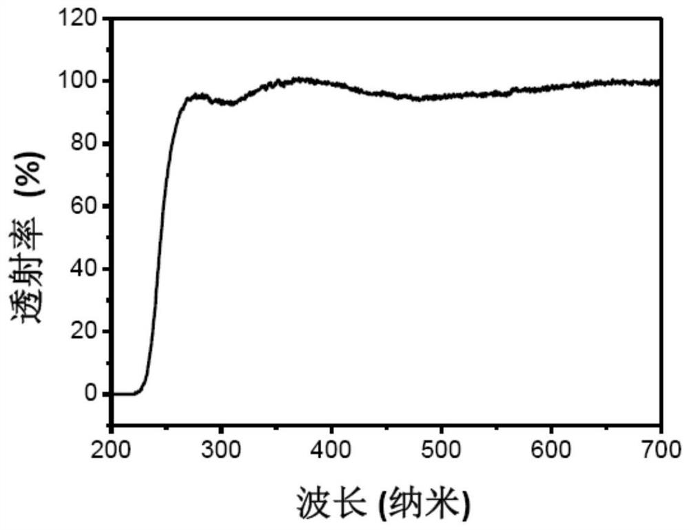
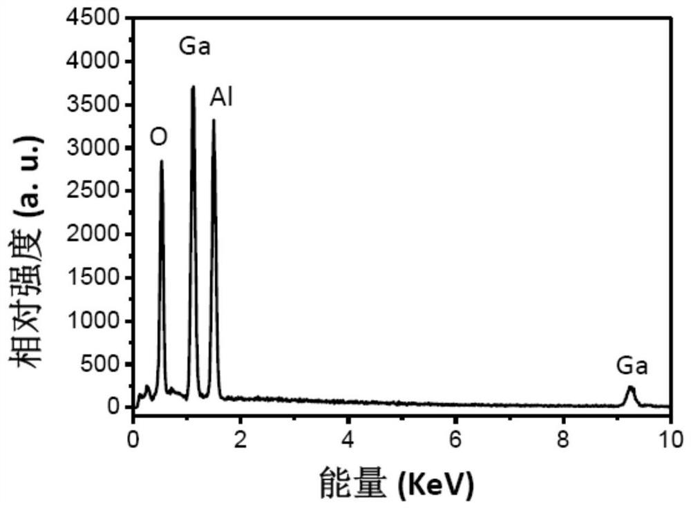
[0054] After testing, it was found that the 4 groups of samples were Ga 2 o 3 The light absorption cut-off edge of the thin film is around 250nm. Except for a small amount of magnesium element detected in the EDS data of samples 2-4, no magnesium element was detected in other samples.

[0055] After the four groups of samples were prepared as ultraviolet detectors, except for sample 2-1, which had no obvious effect on the response time of the device, the response time of the device for other samples was significantly shortened.


PUM


Abstract

The invention provides a preparation method of a Ga2O3 film, which comprises the following steps of by using an organic gallium compound as a gallium source and high-purity oxygen as an oxygen source,carrying out deposition on the surface of a substrate by using a metal organic chemical vapor deposition method, and cooling to obtain the Ga2O3 film, and intermittently supplementing an organic magnesium compound in the growth process of the Ga2O3 film. The invention also provides the Ga2O3 film prepared by the preparation method. The Ga2O3 film is doped with a trace amount of magnesium. By controlling the introduction time and introduction duration of the organic magnesium compound in the preparation of the Ga2O3 film, the preparation of the trace magnesium doped Ga2O3 film is realized, anda convenient and effective means is provided for realizing a high-performance solar blind ultraviolet light detector.

Description

technical field [0001] The invention relates to the field of semiconductor technology, in particular to a Ga 2 o 3 Thin films and methods for their preparation. Background technique [0002] Ultraviolet detection technology is another new military-civilian dual-use detection technology developed after laser and infrared detection technology. It is currently playing a huge role in many fields such as missile tail flame detection, space detection, flame detection and space communication. Especially for detectors working in the sun-blind band (200-280nm), the sensitivity is greatly improved due to the absence of solar ultraviolet interference. In recent years, wide-bandgap semiconductor ultraviolet detectors are considered to be the third-generation ultraviolet detectors that can replace vacuum photomultiplier tubes and Si photomultiplier tubes because of their small size, light weight, no need for filters, and no refrigeration. device. [0003] Ga 2 o 3 As a new type of ...

Claims


Application Information

Patent Timeline
Patent Type & Authority Applications(China)
IPC IPC(8): H01L21/02H01L31/032C23C16/40
CPCC23C16/40H01L21/0242H01L21/02565H01L21/0257H01L21/0262H01L31/0321
Inventor 陈星刘可为申德振李炳辉张振中
Owner CHANGCHUN INST OF OPTICS FINE MECHANICS & PHYSICS CHINESE ACAD OF SCI
Why Eureka
Try Eureka