Homotype heterostructure IMPATT diode and manufacturing method thereof

A heterostructure, diode technology, applied in diodes, semiconductor/solid-state device manufacturing, electrical components, etc., can solve the problems of high ambient temperature, affecting IMPATT output efficiency, large reverse leakage, etc., and achieve the effect of high conversion efficiency

Active Publication Date: 2020-10-02
陕西君普新航科技有限公司
View PDF5 Cites 0 Cited by
  • Summary
  • Abstract
  • Description
  • Claims
  • Application Information

AI Technical Summary

Problems solved by technology

When the concentration is greater than a certain value, the DC-AC conversion efficiency of the device will reach a certain saturation value, and the IMPATT avalanche process will cause saturation of electron-hole pairs due to the limitation of doping concentration, which will affect the output efficiency of IMPATT
[0004] If the Schottky junction is us

Method used


Image

  • Homotype heterostructure IMPATT diode and manufacturing method thereof
  • Homotype heterostructure IMPATT diode and manufacturing method thereof
  • Homotype heterostructure IMPATT diode and manufacturing method thereof

Examples


Embodiment Construction

[0035] The present invention will be described in further detail below in conjunction with specific examples, but not as a limitation of the present invention.

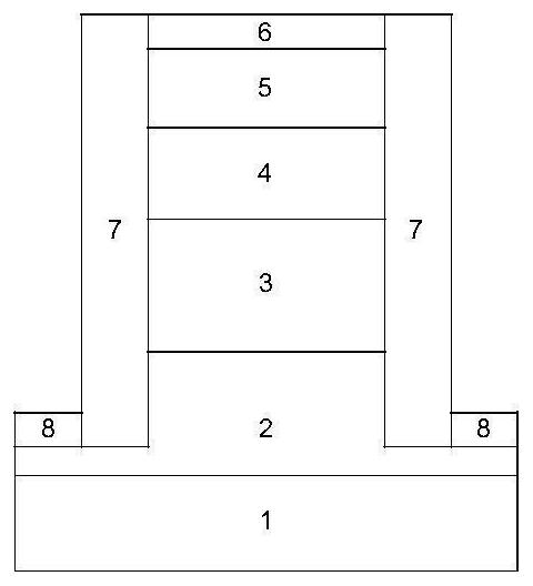
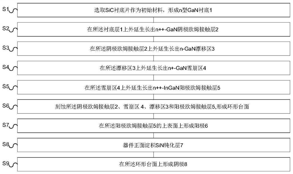
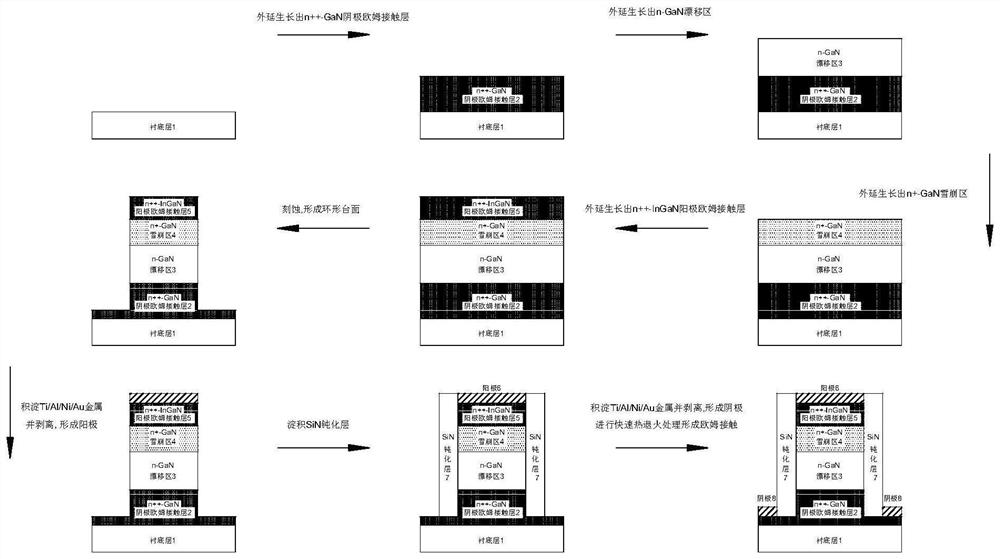
[0036] Such as figure 1 As shown, the same-type heterostructure IMPATT diode of the present invention includes an n-type GaN substrate 1, an n++-GaN cathode ohmic contact layer 2, an n-GaN drift region 3, and an n+-GaN avalanche region 4 arranged sequentially from bottom to top , n++-InGaN anode ohmic contact layer 5 and anode 6.

[0037] The passivation layer 7 is located outside the anode 6 , and the cathode 8 is located on the upper layer of the annular mesa formed by the n++-GaN cathode ohmic contact layer 2 and outside the passivation layer 7 .

[0038] In particular, the n-type GaN substrate 1, as the physical support layer of the device structure layer, not only perfectly matches the upper GaN multilayer structure, thereby significantly improving the crystal quality, but also plays a role in heat dissipation, ...


PUM

PropertyMeasurementUnit
Thicknessaaaaaaaaaa
Doping concentrationaaaaaaaaaa
Thicknessaaaaaaaaaa

Abstract

The invention discloses a homotype heterostructure IMPATT diode and a manufacturing method thereof. The IMPATT diode comprises an n-type GaN substrate, an n++-GaN cathode ohmic contact layer, an n-GaNdrift region, an n+-GaN avalanche region, an n++-InGaN anode ohmic contact layer and an anode which are sequentially arranged from bottom to top. The passivation layer is located outside the anode, and the cathode is located on the upper layer of an annular table top formed by the n++-GaN cathode ohmic contact layer2 and located outside the passivation layer. Compared with a traditional GaN-basedIMPATT diode, the homotype heterostructure IMPATT diode adopting the homotype heterogeneous material has the advantages that the limitation of a P-type GaN doping process is avoided, the efficiency of the IMPATT diode is linearly improved along with the increase of the doping concentration of an InGaN material, and high conversion efficiency is realized; according to the invention, n-type semiconductor materials are adopted, i.e., n-type doping is adopted, so that the efficiency of the manufacturing process is improved, the manufacturing cost is reduced, and meanwhile, the manufacturing process is completely compatible with the traditional IMPATT diode packaging process.

Description

technical field [0001] The invention belongs to the technical field of semiconductors, and relates to a homogeneous heterostructure IMPATT diode and a manufacturing method thereof. Background technique [0002] IMPATT devices with various structures are widely used as the main emission source in a wide frequency range (1-400GHz). The maximum output power of an IMPATT diode at a given frequency has a great relationship with the material properties of the materials used. Compared with traditional semiconductor materials (Si and GaAs), GaN has excellent performance in terms of frequency and output power, and GaN-based IMPATT diodes have broad application prospects in the terahertz field (100GHz-10THz). [0003] The P-type doping concentration of the PN junction in the design of traditional GaN-based IMPATT devices has a great influence on the working performance. P-type GaN is difficult to form high-quality P-type ohmic contacts because of the immature manufacturing technolog...

Claims


Application Information

Patent Timeline
IPC IPC(8): H01L29/864H01L29/207H01L29/205H01L29/20H01L21/329
CPCH01L29/2003H01L29/205H01L29/207H01L29/66219H01L29/864
Inventor 戴扬卢昭阳雷晓艺张云尧廖晨光张涵贠江妮马晓龙赵武张志勇陈晓江
Owner 陕西君普新航科技有限公司
Why Eureka
Try Eureka