Array substrate and display panel

An array substrate and substrate substrate technology, applied in semiconductor devices, electrical components, circuits, etc., can solve problems such as unstable electrical performance of driving circuits, and achieve the goal of improving carrier mobility, reducing costs, and solving threshold voltage drift. Effect

Active Publication Date: 2020-10-09
HEFEI VISIONOX TECH CO LTD
View PDF5 Cites 7 Cited by
  • Summary
  • Abstract
  • Description
  • Claims
  • Application Information

AI Technical Summary

Problems solved by technology

However, the metal oxide thin film transistor in the existing array substrate has a single gate structure, which leads to unstable electrical performance of the driving circuit on the array substrate.

Method used


Image

  • Array substrate and display panel
  • Array substrate and display panel
  • Array substrate and display panel

Examples


Embodiment Construction

[0049] The present invention will be further described in detail below in conjunction with the accompanying drawings and embodiments. It should be understood that the specific embodiments described herein are only used to explain the present invention, but not to limit the present invention. In addition, it should be noted that, for the convenience of description, the drawings only show some but not all structures related to the present invention.

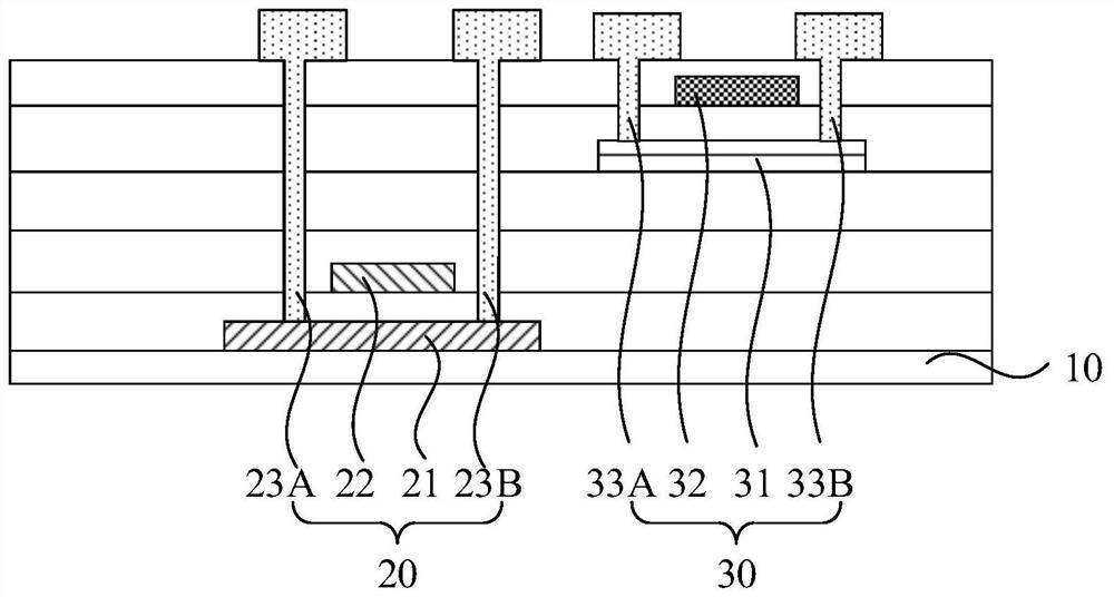
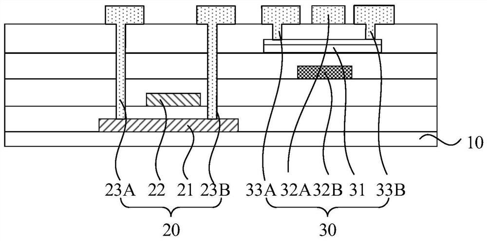
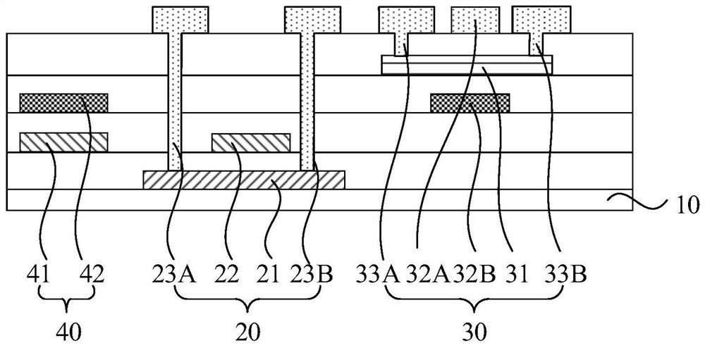
[0050] As described in the background art, the electrical performance of the driving circuit on the existing array substrate is unstable. figure 1 It is a schematic structural diagram of an array substrate in the prior art. see figure 1 The reason is that the existing array substrate includes a base substrate 10; a first thin film transistor 20 and a second thin film transistor 30 located on one side of the base substrate 10; the active layer 21 of the first thin film transistor 20 is low temperature polysilicon, The active laye...


PUM


Abstract

The invention discloses an array substrate and a display panel. The array substrate comprises a substrate, wherein at least one first thin film transistor and at least one second thin film transistorare positioned on one side of the substrate; an active layer of the first thin film transistor is low-temperature polycrystalline silicon, and an active layer of the second thin film transistor is anoxide semiconductor; a gate electrode of the second thin film transistor comprises a top gate electrode and a bottom gate electrode, and the top gate electrode and the bottom gate electrode are connected through a via hole; the gate electrode of the first thin film transistor and a gate electrode of the second thin film transistor are located on different layers; and a source electrode and a drainelectrode of the first thin film transistor, a source electrode and a drain electrode of the second thin film transistor and the top gate electrode are located on the same layer. According to the array substrate provided by the embodiment of the invention, the stability of the electrical property of a driving circuit on the array substrate is improved through the second thin film transistor withthe double-gate structure.

Description

technical field [0001] Embodiments of the present invention relate to the technical field of semiconductors, and in particular, to an array substrate and a display panel. Background technique [0002] With the rapid development of the information technology era, display panels are more and more widely used in display devices such as smartphones, tablet computers, and notebook computers. [0003] A drive circuit of a display unit on an array substrate in a display panel in the prior art includes a low temperature polysilicon thin film transistor and a metal oxide thin film transistor. The metal oxide thin film transistor uses the metal oxide semiconductor layer as the active layer material of the thin film transistor because of its high carrier mobility, low deposition temperature and high optical properties of transparency. Low-temperature polysilicon thin-film transistors have the advantages of high switching speed, thin-film circuits can be made thinner and smaller, and p...

Claims


Application Information

Patent Timeline
Patent Type & Authority Applications(China)
IPC IPC(8): H01L27/12H01L27/32
CPCH01L27/1214H01L27/1251H01L27/1222H10K59/12
Inventor 刘家昌袁鑫曹曙光
Owner HEFEI VISIONOX TECH CO LTD
Why Eureka
Try Eureka