JTE and buried FLR composite terminal structure power device and preparation method thereof

A power device and compound terminal technology, which is applied in semiconductor/solid-state device manufacturing, semiconductor devices, electrical components, etc., can solve problems such as large chip area, affecting device breakdown voltage and reliability, and affecting device surface electric field distribution. The effect of simple process

Active Publication Date: 2020-10-09
BEIJING CENTURY GOLDRAY SEMICON CO LTD
View PDF6 Cites 3 Cited by
  • Summary
  • Abstract
  • Description
  • Claims
  • Application Information

AI Technical Summary

Problems solved by technology

[0004] However, due to the high surface electric field of SiC devices, in order to improve the withstand voltage, it is necessary to reduce the surface peak electric field during device design, and it is necessary to design a large number of field limiting loops.
In the design, many factors such as the number of rings, ring width, and ring spacing will affect the surface electric field distribution, and the terminals of multiple field-limiting rings occupy a large chip area, which is not conducive to increasing the current.
However, the junction terminal extension structure JTE has a figure of merit concentration, and the breakdown withstand voltage of the device terminal is sensitive to the figure of merit concentration of JTE, so the design window is small
Moreover, the junction terminal extension structure is very sensitive to surface charges, and it is easy to affect the electric field distribution on the surface of the device due to interface instability and oxide layer charges, thereby affecting the breakdown voltage and reliability of the device.

Method used


Image

  • JTE and buried FLR composite terminal structure power device and preparation method thereof
  • JTE and buried FLR composite terminal structure power device and preparation method thereof
  • JTE and buried FLR composite terminal structure power device and preparation method thereof

Examples


Embodiment Construction

[0034] The present invention will now be described more fully with reference to the accompanying drawings, in which exemplary embodiments of the invention are shown. This invention may, however, be embodied in many different forms and should not be construed as limited to the exemplary embodiments set forth herein. Rather, these embodiments are provided so that this disclosure will be thorough and complete, and will fully convey the scope of the invention to those skilled in the art.

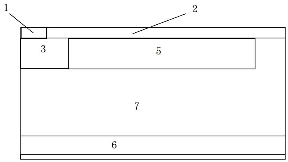
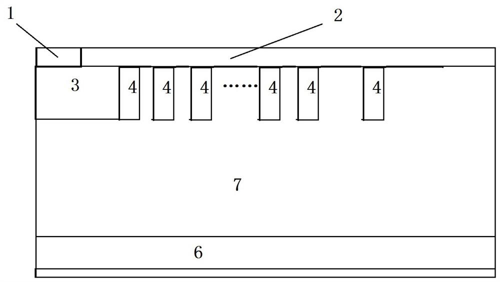
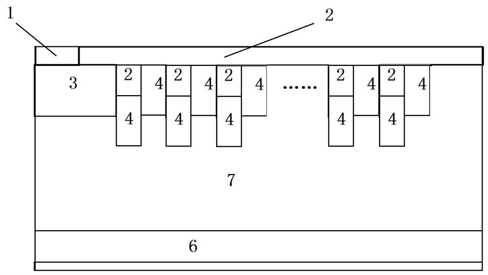
[0035] Such as image 3 As shown, the power device in the embodiment is composed of three structures: the upper layer of the junction terminal region of the N-type epitaxial voltage withstand layer is a P-type layer oppositely doped with the epitaxial layer 7, and at the same time in the upper P-type layer There are discrete multiple trench rings filled with SiO 2 or other High-K dielectrics 2; directly below each trench, there is a P-type ring buried field-limited ring structure oppositely do...


PUM


Abstract

The invention discloses a power device JTE and buried FLR composite terminal structure and a preparation method thereof. The novel terminal structure is mainly formed by combining three structures: anupper layer of a junction terminal region of an N-type (or P-type) epitaxial voltage-withstanding layer is a P-type layer (when the epitaxy is P-type, the P-type layer is N-type) which is doped opposite to the epitaxial layer, a plurality of discrete groove rings are arranged in the upper P-type layer, and SiO2 or other High-K media are filled in grooves; a P-type ring buried field limiting ringstructure which is doped opposite to the epitaxial layer is further arranged under each groove, the upper portions of the P-type rings are connected with the P-type layer on the upper layer, and therefore the composite structure voltage-withstanding terminal with the JTE structure on the upper layer and the FLR on the lower layer is formed. The composite terminal is simple in structure and process, is not sensitive to JTE concentration or process deviation of FLR ring width and spacing and surface charges, and can greatly improve the voltage endurance capability of the device terminal and reduce the chip area of the required voltage endurance terminal.

Description

technical field [0001] The invention relates to the technical field of semiconductor devices, in particular to a JTE and FLR compound terminal structure of a power device and a preparation method thereof. Background technique [0002] SiC is a wide bandgap semiconductor material that has developed rapidly in the past ten years. Compared with other semiconductor materials, such as Si, GaN and GaAs, SiC material has wide bandgap, high thermal conductivity, high carrier saturation mobility, high power density and other advantages. SiC can be thermally oxidized to form silicon dioxide, making it possible to realize power devices and circuits such as SiC MOSFET, SBD, IGBT and GTO. Since the 1990s, power devices such as SiC MOSFETs and SBDs have been widely used in switching regulated power supplies, high-frequency heating, automotive electronics, and power amplifiers. [0003] At present, in the design and fabrication process of silicon carbide power devices, especially high-vo...

Claims


Application Information

Patent Timeline
Patent Type & Authority Applications(China)
IPC IPC(8): H01L29/06H01L21/329
CPCH01L29/0623H01L29/0684H01L29/0649H01L29/6606
Inventor 袁俊徐妙玲黄兴倪炜江孙安信
Owner BEIJING CENTURY GOLDRAY SEMICON CO LTD
Why Eureka
Try Eureka