3D chip signal coupling analysis system and method based on machine learning

A technology of signal coupling and machine learning, applied in neural learning methods, instruments, computer-aided design, etc., can solve problems such as less research on inductive coupling methods, and achieve high accuracy, high accuracy, and flexible analysis

Active Publication Date: 2020-10-16
ZHEJIANG UNIV
View PDF5 Cites 4 Cited by
  • Summary
  • Abstract
  • Description
  • Claims
  • Application Information

AI Technical Summary

Problems solved by technology

[0004] However, there are some key technical difficulties in the TSV three-dimensional integration process and design, such as

Method used


Image

  • 3D chip signal coupling analysis system and method based on machine learning
  • 3D chip signal coupling analysis system and method based on machine learning
  • 3D chip signal coupling analysis system and method based on machine learning

Examples


Embodiment Construction

[0032] The specific embodiments of the present invention will be further described below in conjunction with the accompanying drawings.

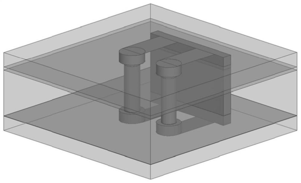
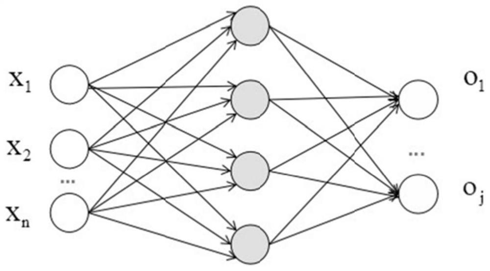
[0033] The present invention proposes a 3D chip signal coupling analysis system based on machine learning, which includes a 3D model of a TSV through hole, an RLGC equivalent circuit model of a TSV through hole, and a BP neural network; the TSV through hole is in a 3D chip Through silicon channels that carry signals between layers.

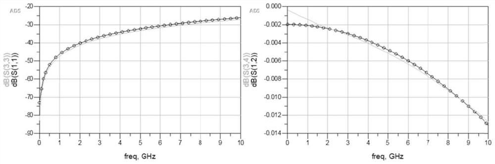
[0034] Such as figure 1 As shown, the 3D model of the TSV through-hole is constructed and simulated using HFSS software, and the energy dissipation and transmission capacity of the model are used as indicators for analysis. Among all the design size parameters, the design parameters that have a greater impact on the indicators are selected, including TSV length, TSV diameter, and TSV spacing, as the main influencing factors. Considering the ideal 3D model of TSV through-holes, only the influence of TSV on its ...


PUM


Abstract

The invention discloses a 3D chip signal coupling analysis system and method based on machine learning, and the method comprises the steps of obtaining S parameters of TSV through holes under different radius and height of the TSV through holes and distance parameters between the through holes through a TSV through hole 3D model, and respectively storing the S parameters into an S2P file; buildinga TSV through hole RLGC equivalent circuit model, and obtaining circuit parameters of the RLGC equivalent circuit under the corresponding size according to the S2P file; using the radius and the height of the TSV through holes and the distance parameters between the through holes as the input of the BP neural network; and taking the circuit parameters of the RLGC equivalent circuit as the outputof the BP neural network, training the BP neural network, and performing S parameter simulation analysis according to the output of the trained network to obtain an analysis result which is the transmission characteristics of the TSV 3D model under the corresponding size. According to the neural network, actual model simulation and optimization results are adopted as a training set, analysis of circuit performance under different conditions is more flexible, and higher accuracy is achieved.

Description

technical field [0001] The invention relates to the field of 3D chip signal transmission, in particular to a machine learning-based 3D chip signal coupling analysis system and method, which can quickly and accurately obtain the equivalent circuit of a 3D model by using the machine learning method. [0002] technical background [0003] As electronic components and PCB manufacturing continue to encounter obstacles on the road to try to reduce the size, it is necessary for related equipment to achieve more functions at a higher speed in a smaller dimension, and Moore's Law is becoming more and more unsustainable. Engineers found that the existing packaging technology is limited to a single plane, and cannot continue to move towards the goal of doubling the integration level every 18 months. 3D chips are considered to be a solution to the bottleneck of Moore's Law, so the demand for 3D chips is increasing strong. 3D chips have shorter transmission distances, higher performance,...

Claims


Application Information

Patent Timeline
IPC IPC(8): G06F30/3323G06N3/04G06N3/08
CPCG06F30/3323G06N3/08G06N3/044G06N3/045
Inventor 张力唐思瑶施叶昕李原
Owner ZHEJIANG UNIV
Why Eureka
Try Eureka