Semiconductor device and preparation method thereof

A semiconductor and device technology, which is applied in the field of semiconductor devices and their preparation, can solve the problems of high preparation cost and unfavorable laser promotion, and achieve the effects of reducing preparation cost, reducing preparation difficulty, and preventing transmission loss

Pending Publication Date: 2020-10-16
UNITED MICROELECTRONICS CENT CO LTD
View PDF3 Cites 0 Cited by
  • Summary
  • Abstract
  • Description
  • Claims
  • Application Information

AI Technical Summary

Problems solved by technology

However, when using a silicon-on-insulator wafer to prepare the laser, higher manufacturing costs are required, which is not conducive to the promotion of the laser.

Method used


Image

  • Semiconductor device and preparation method thereof
  • Semiconductor device and preparation method thereof
  • Semiconductor device and preparation method thereof

Examples


preparation example Construction

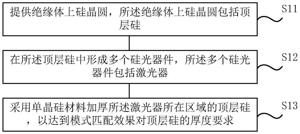
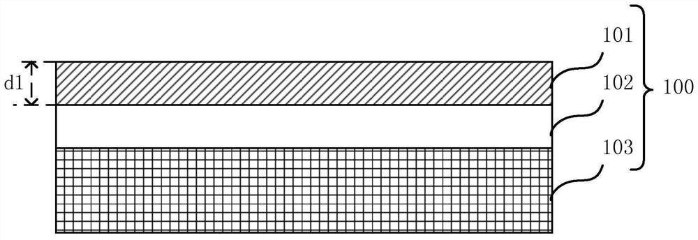
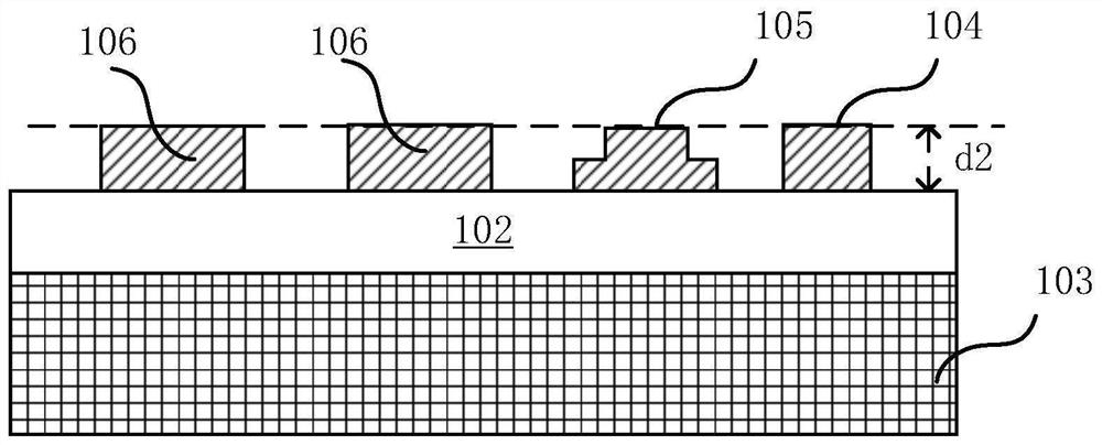
[0033] In this specific embodiment, a method for manufacturing a semiconductor device is provided, including the following steps: S11 provides a silicon-on-insulator wafer 100, the silicon-on-insulator wafer 100 includes a top-layer silicon 101, please refer to figure 2 ; S12 forms a plurality of silicon photonic devices in the top layer silicon 101 (the silicon photonic devices include all components shown in labels 104, 105, and 106), and the silicon photonic devices include a laser 106, please refer to here image 3 ; S13 uses single crystal silicon material to thicken the top layer silicon 101 in the region where the laser is located, to achieve the mode matching effect on the thickness requirements of the top layer silicon 101, please refer to here Figure 7 .

[0034] In this specific embodiment, in the manufacturing method of the semiconductor device, the top layer of silicon 101 in the area where the laser 106 is located is thickened by using single crystal silicon ma...


PUM

PropertyMeasurementUnit
thicknessaaaaaaaaaa
thicknessaaaaaaaaaa
thicknessaaaaaaaaaa

Abstract

The invention discloses a semiconductor device and a preparation method thereof, and the method comprises the following steps: providing a silicon-on-insulator wafer which comprises top silicon; forming a plurality of silicon optical devices in the top silicon, wherein the plurality of silicon optical devices comprise lasers; and thickening the top silicon of the area where the laser is located soas to meet the requirement of the mode matching effect on the thickness of the top silicon.

Description

technical field [0001] The invention relates to the field of semiconductor preparation, in particular to a semiconductor device and a preparation method thereof. Background technique [0002] The silicon photonics process on the silicon-on-insulator wafer itself has a relatively complete set of optical components, including various passive devices, electro-optic modulators, and photodetectors. However, as an indirect bandgap material, silicon cannot directly emit light, which makes the integration of silicon-based light sources one of the important challenges in the development of silicon-based optoelectronics technology. [0003] In the prior art, lasers are often fabricated using a silicon photonics process on a silicon-on-insulator wafer. However, when the laser is prepared by using a silicon-on-insulator wafer, relatively high preparation costs are required, which is unfavorable for popularization of the laser. Contents of the invention [0004] The invention provide...

Claims


Application Information

Patent Timeline
Patent Type & Authority Applications(China)
IPC IPC(8): H01L21/762H01L21/84
CPCH01L21/7624H01L21/84
Inventor 刘思旸朱继光冯俊波
Owner UNITED MICROELECTRONICS CENT CO LTD
Why Eureka
Try Eureka