Wafer-level thin film packaging method and packaging device

A thin-film packaging and packaging method technology is applied in the field of wafer-level thin-film packaging methods and packaging devices, and can solve the problems of complex process process and high process temperature of micromechanical vacuum packaging technology

Pending Publication Date: 2020-10-20
SHANGHAI INST OF MICROSYSTEM & INFORMATION TECH CHINESE ACAD OF SCI
View PDF21 Cites 0 Cited by
  • Summary
  • Abstract
  • Description
  • Claims
  • Application Information

AI Technical Summary

Problems solved by technology

[0005] The technical problem to be solved by the present invention is that the existing micro-mechanical vacuum packaging technology has the problems of high process temperature and complicated process

Method used


Image

  • Wafer-level thin film packaging method and packaging device
  • Wafer-level thin film packaging method and packaging device
  • Wafer-level thin film packaging method and packaging device

Examples


Embodiment 1

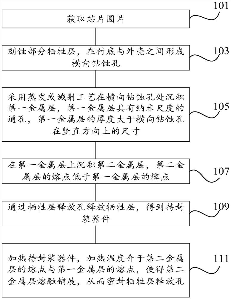
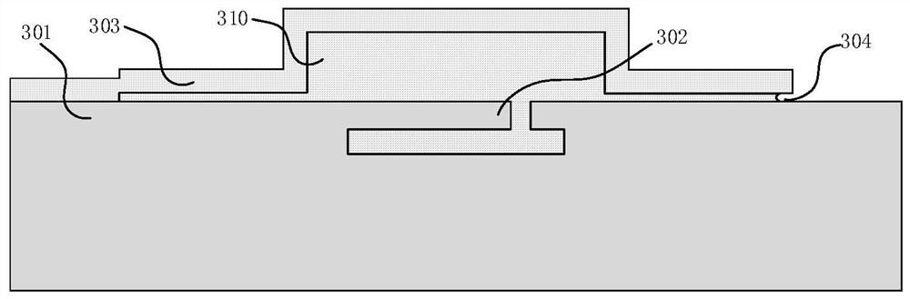
[0129] In this embodiment, the sacrificial layer 310 is made of thermally oxidized SiO 2 The shell 303 is made of LPCVD polysilicon, the sacrificial layer 310 is made of lateral drilled holes 304 by SiO2 (before metal) wet etching process, the first metal layer 306 is made of metal sputtering TiWu / Cu, and self-aligned to form nano-through The holes 307 and the second metal layer 308 are made of electroplated lead-free tin. The specific steps are:

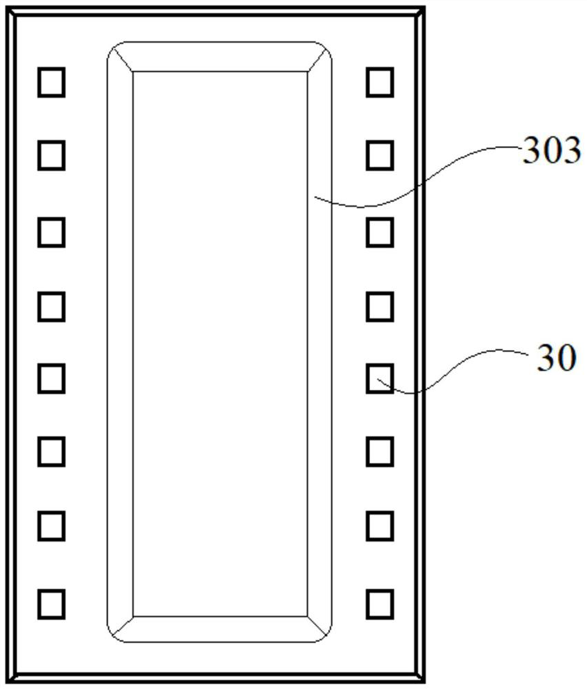
[0130] Fabricating Micromechanical Structures 302: AS Figure 16 As shown, the micromechanical structure 302 is fabricated using a conventional bulk micromachining process.

[0131] Make double-layer sacrificial layer 310 structure: such as Figure 16 As shown, the double-layer sacrificial layer 310 structure adopts thermal oxidation SiO 2 fabrication, first using thermally oxidized SiO 2 Making the first sacrificial layer 311, using photolithography, SiO 2 The (pre-metal) wet etching process realizes patterning of the first s...

Embodiment 2

[0141] In this embodiment, the sacrificial layer 310 is made of LPCVD silicon dioxide, the shell 303 is made of micro-electroformed low-stress Ni, and the lateral drill hole 304 on the sacrificial layer 310 is made of SiO 2 (After metal) Wet etching process, the first metal layer 306 is made of metal evaporated Ni / Au, and self-aligned to form nano-vias 307, and the second metal layer 308 is made of metal sputtering Sn. The specific steps are:

[0142] Fabricating Micromechanical Structures 302: AS Figure 27 As shown, the micromechanical structure 302 is fabricated using a conventional bulk micromachining process.

[0143] Make double-layer sacrificial layer 310 structure: such as Figure 27 As shown, the double-layer sacrificial layer 310 structure is made of LPCVD silicon dioxide, firstly using LPCVD SiO 2 Make the first sacrificial layer 311, using photolithography / SiO 2 The (pre-metal) wet etching process realizes patterning of the first sacrificial layer 311 , and the...

Embodiment 3

[0152] In this embodiment, the sacrificial layer 310 structure is made of PECVD silicon dioxide, the shell 303 is made of PECVD polysilicon, the sacrificial layer 310 is made of SiO2 (before metal) wet etching process, and the first metal layer 306 is made of metal It is made by sputtering Ni / Au, and self-aligned to form the nanometer through hole 307, and the second metal layer 308 is made by metal sputtering In. The specific steps are:

[0153] Fabricating Micromechanical Structures 302: AS Figure 36 As shown, the micromechanical structure 302 is fabricated using a conventional bulk micromachining process.

[0154] Make double-layer sacrificial layer 310 structure: such as Figure 36 As shown, the double-layer sacrificial layer 310 structure is made of PECVD silicon dioxide, firstly using PECVD SiO 2 Make the first sacrificial layer 311, utilize the photolithography / SiO2 (before metal) wet etching process to realize the patterning of the first sacrificial layer 311, fina...


PUM

PropertyMeasurementUnit
melting pointaaaaaaaaaa
thicknessaaaaaaaaaa

Abstract

The invention relates to the technical field of micro-electro-mechanical packaging, in particular to a wafer-level thin film packaging method and packaging device. The method comprises the steps of: obtaining a chip wafer; etching a part of a sacrificial layer, and forming a transverse drilling hole between the substrate and the shell; depositing a first metal layer at the transverse drilling andetching hole by adopting an evaporation or sputtering process, wherein the first metal layer is provided with a nanoscale through hole; depositing a second metal layer on the first metal layer; releasing the sacrificial layer through the sacrificial layer release hole to obtain a to-be-packaged device; and heating the to-be-packaged device at a heating temperature between the melting point of thesecond metal layer and the melting point of the first metal layer to melt and spread the second metal layer so as to seal the sacrificial layer release hole. The packaging structure is provided with the transverse drilling and etching holes, the transverse drilling and etching holes are used for forming the self-aligning through holes in the metal layer, and sealing can be achieved by depositing asmall amount of low-melting-point sealing metal at the through holes.

Description

technical field [0001] The invention relates to the technical field of microelectronic mechanical packaging, in particular to a wafer-level thin film packaging method and a packaging device. Background technique [0002] Micro-Electro-Mechanical System (MEMS) sensors achieve high functional integration by reducing the size of sensitive structures. Air resistance is related to the size of structural features. At low speeds, the air resistance of macroscopic objects is generally negligible. However, in MEMS sensors with small structural feature scales, air resistance is the main damping mechanism of MEMS devices, which determines the Q value of the sensor. , which has a significant impact on the amplitude-frequency characteristics, phase-frequency characteristics and bandwidth of the sensor. At the same time, the Brownian motion noise caused by the thermal fluctuation of gas molecules is also the main noise of MEMS devices such as acceleration sensors and gyroscopes. Vacuum ...

Claims


Application Information

Patent Timeline
Patent Type & Authority Applications(China)
IPC IPC(8): B81C1/00B81B7/00
CPCB81C1/00095B81C1/00261B81B7/0006B81B7/0032
Inventor 钟朋裴彬彬孙珂杨恒李昕欣
Owner SHANGHAI INST OF MICROSYSTEM & INFORMATION TECH CHINESE ACAD OF SCI
Why Eureka
Try Eureka