Supercharge Your Innovation With Domain-Expert AI Agents!

Process for processing TGV by combining femtosecond laser with HF wet etching

A femtosecond laser and wet etching technology, applied in laser welding equipment, metal processing equipment, manufacturing tools, etc., can solve problems such as poor processing rate, inability to withstand huge stress, and weakened strength

Pending Publication Date: 2020-10-20
绍兴同芯成集成电路有限公司
View PDF0 Cites 2 Cited by
  • Summary
  • Abstract
  • Description
  • Claims
  • Application Information

AI Technical Summary

Problems solved by technology

However, this process has the following disadvantages: (1) when the perforation area is large, the laser scanning time is long, and the processing rate is poor; (2) the strength of the support plate itself is greatly weakened after the glass carrier is scanned and perforated. Afterwards, the thinning and grinding process of the wafer cannot bear the huge stress; (3) After the hole is completely perforated, when the bonding layer must be coated with a releasing layer or an adhesive layer on the glass carrier, solvents and Coating material will slip through the perforations or partially adhere to the perforations, causing problems with coating uniformity

Method used


Image

  • Process for processing TGV by combining femtosecond laser with HF wet etching
  • Process for processing TGV by combining femtosecond laser with HF wet etching
  • Process for processing TGV by combining femtosecond laser with HF wet etching

Examples


Embodiment 1

[0035] A femtosecond laser combined with HF wet etching process TGV process, comprising the following steps:

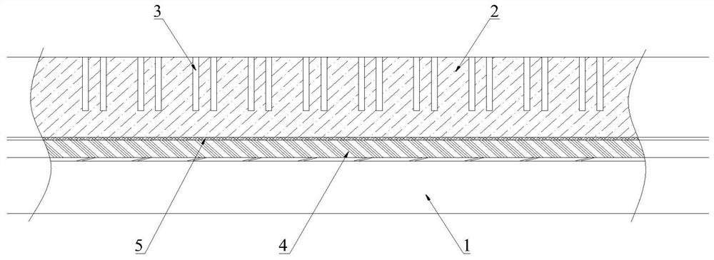
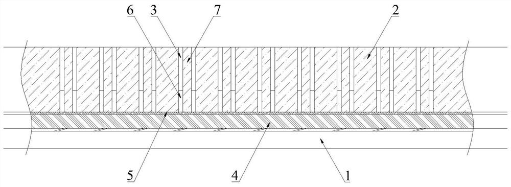
[0036] S1. Permanently bond the front of the wafer to the glass carrier, then turn it over to the glass surface, scan the surrounding area of ​​the hole on the glass carrier with a femtosecond laser, deconstruct the glass bond in this area, and use HF to etch the area to form a circular etching hole , the depth of the etched hole is 85% of the thickness of the glass substrate, the central wavelength of the femtosecond laser is 810nm, and the pulse width is 320×10 -15 s, the repetition frequency is 100kHz;

[0037] S2. Turn over to the wafer side, and perform thinning and component engineering on the back side of the wafer;

[0038] S3, turn over to the glass surface again, and use HF etching to perform the second pattern etching process until the perforation is completed;

[0039] S4. Use laser to debond the middle island glass area, then put the wafer and glass car...

Embodiment 2

[0042] A femtosecond laser combined with HF wet etching process TGV process, comprising the following steps:

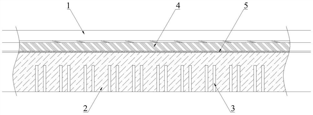
[0043] S1. Temporarily bond the front of the wafer to a glass carrier, then turn it over to the glass surface, scan the surrounding area of ​​the hole on the glass carrier with a femtosecond laser, deconstruct the glass bond in this area, and use HF to etch this area to form a circular etching hole. , the depth of the etched hole is 80% of the thickness of the glass substrate, the central wavelength of the femtosecond laser is 780nm, and the pulse width is 92×10 -15 s, the repetition frequency is 85kHz;

[0044] S2. Flip over to the wafer side, and perform thinning and component engineering on the back side of the wafer;

[0045] S3, turn over to the glass surface again, and use HF etching to perform the second pattern etching process until the perforation is completed;

[0046]S4. Use laser to debond the middle island glass area, then put the wafer and glass carrie...


PUM

PropertyMeasurementUnit
Wavelengthaaaaaaaaaa
Pulse widthaaaaaaaaaa

Abstract

The invention discloses a process for processing TGV by combining femtosecond laser with HF wet etching. The process comprises the following steps: S1, bonding a wafer with a glass carrier plate, scanning the periphery of a hole in a glass surface by using femtosecond laser, and etching an annular etching hole by using HF; S2, carrying out thinning and element engineering on the back surface of the wafer; S3, performing secondary pattern etching processing on the glass surface by applying HF etching to finish perforation; S4, stripping the glass in a middle island area to complete the overallTGV penetration; and S5, etching an adhesion layer and a release layer by using O2 Plasma plasma, enabling the TGV to be completely communicated with the front surface of the wafer, and continuously manufacturing chemical plating and metal electroplating processes. According to the invention, the femtosecond laser is combined with HF wet etching; the perforated glass carrier plate is formed by etching twice, the influence of the overall strength is extremely small, the stress during grinding can still be borne, the coating surface is smooth, a circle of glass structure bonding on the peripheryof a hole is deconstructed through femtosecond laser, the machining area is greatly reduced, the efficiency is improved, and a double-sided machining process can be carried out.

Description

technical field [0001] The invention relates to the field of semiconductors, in particular to a femtosecond laser combined with HF wet etching process for TGV processing. Background technique [0002] With the rise of communication electronics, people's demand for miniaturized and high-sensitivity modules or systems is getting higher and higher, and the requirements for signal quality are becoming more and more stringent. High-density integration technologies, such as System-in-Package (SiP) technologies, have developed rapidly, but miniaturized integrated packaging of mixed-signal multi-chip systems has become one of the technical difficulties in this field. The new 3D packaging technology represented by system-in-package, in addition to technologies such as three-dimensional chip stacking (Stacked Diepackage), package stacking (Package on Package, POP), the application of some new materials and new technologies brings opportunities for packaging miniaturization, For examp...

Claims


Application Information

Patent Timeline
IPC IPC(8): H01L21/306H01L21/48B23K26/352
CPCH01L21/30604H01L21/486B23K26/352
Inventor 严立巍陈政勋李景贤
Owner 绍兴同芯成集成电路有限公司
Features
  • R&D
  • Intellectual Property
  • Life Sciences
  • Materials
  • Tech Scout
  • Unparalleled Data Quality
  • Higher Quality Content
  • 60% Fewer Hallucinations
Learn More