Supercharge Your Innovation With Domain-Expert AI Agents!

A kind of double-sided thick film electroplating copper heat dissipation structure manufacturing method

A technology of heat dissipation structure and manufacturing method, which is applied in the direction of circuits, electrical components, and electrical solid devices, and can solve problems such as difficult and complicated operation processes, achieve low cost, solve excessive stress, increase mass production and yield Effect

Active Publication Date: 2021-12-28
绍兴同芯成集成电路有限公司
View PDF6 Cites 0 Cited by
  • Summary
  • Abstract
  • Description
  • Claims
  • Application Information

AI Technical Summary

Problems solved by technology

It solves the problem that the production of double-sided thick-film copper heat sinks or pillars combined with ultra-thin wafers is difficult and the actual operation process is complicated.

Method used


Image

  • A kind of double-sided thick film electroplating copper heat dissipation structure manufacturing method
  • A kind of double-sided thick film electroplating copper heat dissipation structure manufacturing method
  • A kind of double-sided thick film electroplating copper heat dissipation structure manufacturing method

Examples


Embodiment 1

[0079] A method for manufacturing a double-sided thick-film electroplating copper heat dissipation structure, comprising the following steps:

[0080] S1: Surface treatment on the wafer

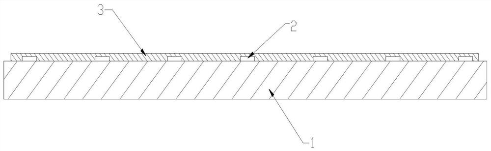
[0081] Perform ion implantation and yellow light process on the upper surface of wafer 1, and make metal contacts 2, such as figure 1 As shown, the thickness of wafer 1 is 700um;

[0082] S2: Depositing thin films

[0083] Surface deposition of SiO on wafer 1 using PEVCD 2 and Si 3 N 4 Film 3, such as figure 2 As shown, the film thickness is 0.5um;

[0084] S3: One polyimide thick film coating

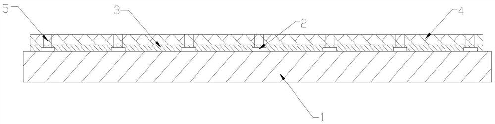
[0085] In SiO 2 and Si 3 N 4 A layer of polyimide thick film 4 is coated on the film 3, and a metal contact window 5 with an area smaller than the area of ​​the metal contact 2 is opened on the metal contact 2 by Mask exposure, such as image 3 As shown, the thickness of the polyimide thick film 4 is 10um, and the polyimide thick film 4 is baked and cured after development;

[0086] S4: E...

Embodiment 2

[0117] A method for manufacturing a double-sided thick-film electroplating copper heat dissipation structure, comprising the following steps:

[0118] S1: Surface treatment on the wafer

[0119] Perform ion implantation and yellow light process on the upper surface of wafer 1, and make metal contacts 2, such as figure 1 As shown, the thickness of wafer 1 is 700um;

[0120] S2: Depositing thin films

[0121] Surface deposition of SiO on wafer 1 using PEVCD 2 and Si 3 N 4 Film 3, such as figure 2 As shown, the film thickness is 1.5um;

[0122] S3: one polyimide thick film coating

[0123] In SiO 2 and Si 3 N 4 A layer of polyimide thick film 4 is coated on the film 3, and a metal contact window 5 with an area smaller than the area of ​​the metal contact 2 is opened on the metal contact 2 by Mask exposure, such as image 3 As shown, the thickness of the polyimide thick film 4 is 15um, and the polyimide thick film 4 is baked and cured after development;

[0124] S4: E...

Embodiment 3

[0155] A method for manufacturing a double-sided thick-film electroplating copper heat dissipation structure, comprising the following steps:

[0156] S1: Surface treatment on the wafer

[0157] Perform ion implantation and yellow light process on the upper surface of wafer 1, and make metal contacts 2, such as figure 1 As shown, the thickness of wafer 1 is 700um;

[0158] S2: Depositing thin films

[0159] Surface deposition of SiO on wafer 1 using PEVCD 2 and Si 3 N 4 Film 3, such as figure 2 Shown, where the film thickness is 1.0um;

[0160] S3: One polyimide thick film coating

[0161] In SiO 2 and Si 3 N 4 A layer of polyimide thick film 4 is coated on the film 3, and a metal contact window 5 with an area smaller than the area of ​​the metal contact 2 is opened on the metal contact 2 by Mask exposure, such as image 3 As shown, the thickness of the polyimide thick film 4 is 20um, and the polyimide thick film 4 is baked and cured after development;

[0162] S4...


PUM


Abstract

The invention discloses a method for manufacturing a double-sided thick-film electroplating copper heat dissipation structure, which includes the following steps: wafer upper surface treatment, thin film deposition, polyimide thick film coating, etching, Cu seed layer plating, flipping, grinding, gentle slope ( step) etching, removal of grinding tape film, wafer lower surface treatment, secondary polyimide thick film coating, primary coating of photoresist, secondary coating of photoresist, copper injection, removal of polyimide thick film, removal of Cu seed layer, placement Wafer, dicing. The double-sided polyimide process of the present invention combined with the double-sided thick-film Cu ECP process can provide ultra-thin wafers combined with double-sided Cu heat sinks (columns), achieving obvious and huge advantages in process feasibility and cost; the front polyimide not only provides perfect components Protection also forms a perfect edge support and stress buffer in combination with production, which greatly improves the feasibility, mass production and yield of ultra-thin wafer production. The invention solves the problems in the prior art that the manufacture of double-sided thick-film copper heat sinks or pillars combined with ultra-thin wafers is difficult and the actual operation process is complicated.

Description

technical field [0001] The invention belongs to the field of electroplating heat dissipation, and in particular relates to a method for manufacturing a double-sided thick-film electroplating copper heat dissipation structure. Background technique [0002] In the prior art, it is extremely difficult to manufacture double-sided thick-film copper heat sinks or pillars combined with ultra-thin wafers. The main difficulty is that the ultra-thin wafers cannot withstand the mechanical actions during the process operation and the huge stress of the thick copper metal film. Although the glass carrier technology can overcome the mechanical limitations of ultra-thin sheets, it is necessary to open the window on the back of the carrier to remove the barrier of the adhesive layer, so that double-sided coating, exposure, development, electroplating, etching and other processes can be carried out. [0003] The patented invention uses polyimide thick films on the front and back sides to for...

Claims


Application Information

Patent Timeline
Patent Type & Authority Patents(China)
IPC IPC(8): H01L21/48H01L23/367
CPCH01L21/4871H01L23/3672
Inventor 严立巍陈政勋李景贤
Owner 绍兴同芯成集成电路有限公司
Features
  • R&D
  • Intellectual Property
  • Life Sciences
  • Materials
  • Tech Scout
  • Unparalleled Data Quality
  • Higher Quality Content
  • 60% Fewer Hallucinations
Learn More