Cross-scale micro-nano structure three-dimensional measurement device and measurement method

A micro-nano structure, three-dimensional measurement technology, applied in the direction of measuring devices, optical devices, instruments, etc., can solve the problems of positioning reference error, data fusion, difficult to find the measured area, etc.

Active Publication Date: 2020-10-30
HUAZHONG UNIV OF SCI & TECH
View PDF9 Cites 6 Cited by
  • Summary
  • Abstract
  • Description
  • Claims
  • Application Information

AI Technical Summary

Problems solved by technology

[0004] Aiming at at least one of the above defects or improvement needs in the prior art, the present invention provides a three-dimensional measurement device for cross-scale micro-nano structures, which can realize large-scale and high-resolution measurement of the surface of cross-scale micro-nano structures, and can The measurement of cross-scale (micron-scale, sub-micron and below-scale) structures can be realized in this set of sy...

Method used


Image

  • Cross-scale micro-nano structure three-dimensional measurement device and measurement method
  • Cross-scale micro-nano structure three-dimensional measurement device and measurement method
  • Cross-scale micro-nano structure three-dimensional measurement device and measurement method

Examples


Embodiment Construction

[0040] In order to make the object, technical solution and advantages of the present invention clearer, the present invention will be further described in detail below in conjunction with the accompanying drawings and embodiments. It should be understood that the specific embodiments described here are only used to explain the present invention, not to limit the present invention. In addition, the technical features involved in the various embodiments of the present invention described below can be combined with each other as long as they do not constitute a conflict with each other. The present invention will be further described in detail below in combination with specific embodiments.

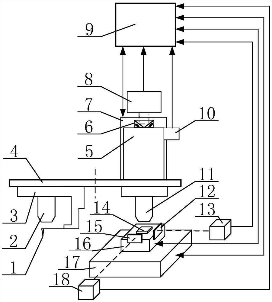
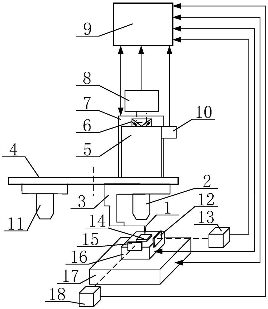
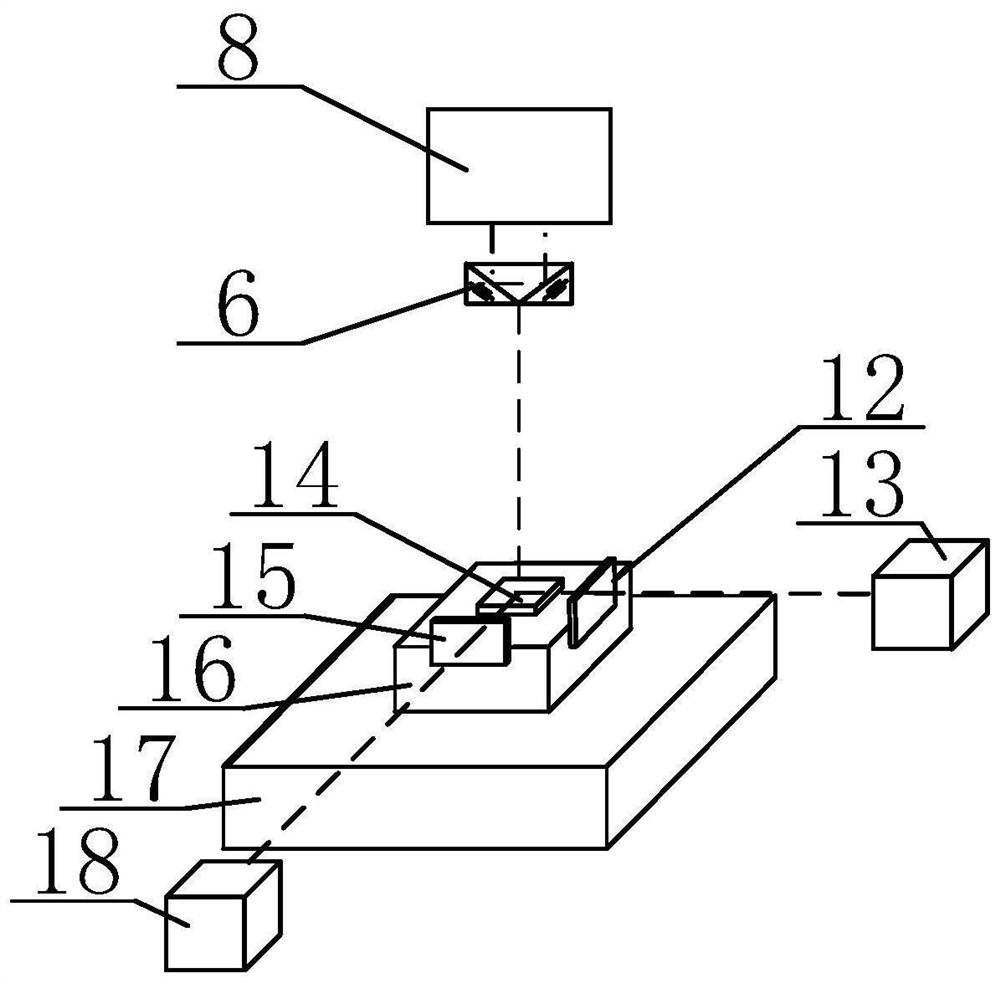
[0041] Such as figure 1 As shown, the present invention provides a three-dimensional measurement device for cross-scale micro-nano structures, which includes: white light interference system 5, nanoscale vertical micro-displacement platform 7, laser interference displacement measurement sys...


PUM


Abstract

The invention discloses a cross-scale micro-nano structure three-dimensional measurement device and a measurement method. The device is characterized by comprising an atomic force probe scanning microscope assembly, an objective lens turntable, a white light interference system, a nanoscale vertical micro-displacement platform, a laser interference displacement metering system I, a measurement andcontrol system, a laser interference displacement metering system II, a sample piece, a two-dimensional piezoelectric ceramic scanning platform, a two-dimensional electric scanning platform and a laser interference displacement metering system III. According to the invention, by rotating the objective lens turntable, the measuring device is switched between a white light interference measuring mode and an atomic force probe scanning measuring mode, wherein the white light interference measuring mode is mainly used for large-scale measurement of a micron-scale structure, and the atomic force probe scanning measuring mode is used for carrying out horizontal high-resolution measurement on the nanoscale feature region, so that large-range and high-resolution measurement on the surface of thecross-scale micro-nano structure is achieved, and measurement of the cross-scale (micron scale, submicron scale and below scale) structure can be achieved in one set of system.

Description

technical field [0001] The invention belongs to the field of ultra-precise surface topography measurement, and in particular relates to a three-dimensional measurement device and method for cross-scale micro-nano structures. Background technique [0002] With the development of advanced manufacturing technologies such as lithography, ultra-precision processing, and optical processing, the surface of cross-scale micro-nano structures has become an important surface feature of key components in the fields of solar cells, laser holographic anti-counterfeiting, and flat-panel displays. The overall macroscopic size of these features is gradually increasing, while the local microscopic features are more refined, resulting in the measurement requirements of both large-scale and high-resolution. Traditional surface topography measurement instruments, such as stylus profilers, optical profilers, atomic force microscopes, etc., have been widely used in ultra-precision surface measurem...

Claims


Application Information

Patent Timeline
IPC IPC(8): G01B11/24G01B11/02G01B9/02
CPCG01B9/02055G01B9/0209G01B11/02G01B11/2441
Inventor 卢文龙刘晓军
Owner HUAZHONG UNIV OF SCI & TECH
Why Eureka
Try Eureka