Semiconductor structure and forming method thereof

A technology of semiconductor and gate structure, which is applied in the field of semiconductor structure and its formation, and can solve the problems of poor overall performance of semiconductor devices

Pending Publication Date: 2020-10-30
SEMICON MFG INT (SHANGHAI) CORP +1
View PDF0 Cites 0 Cited by
  • Summary
  • Abstract
  • Description
  • Claims
  • Application Information

AI Technical Summary

Problems solved by technology

[0004] However, the performance of the SRAM in the semiconductor device formed in the prior art needs to be further improved, so that the overall performance of the semiconductor device is poor

Method used


Image

  • Semiconductor structure and forming method thereof
  • Semiconductor structure and forming method thereof
  • Semiconductor structure and forming method thereof

Examples


Embodiment Construction

[0015] It can be seen from the background art that the devices formed so far still have the problem of poor performance. The reasons for the poor performance of the device are analyzed in conjunction with a method of forming a semiconductor structure.

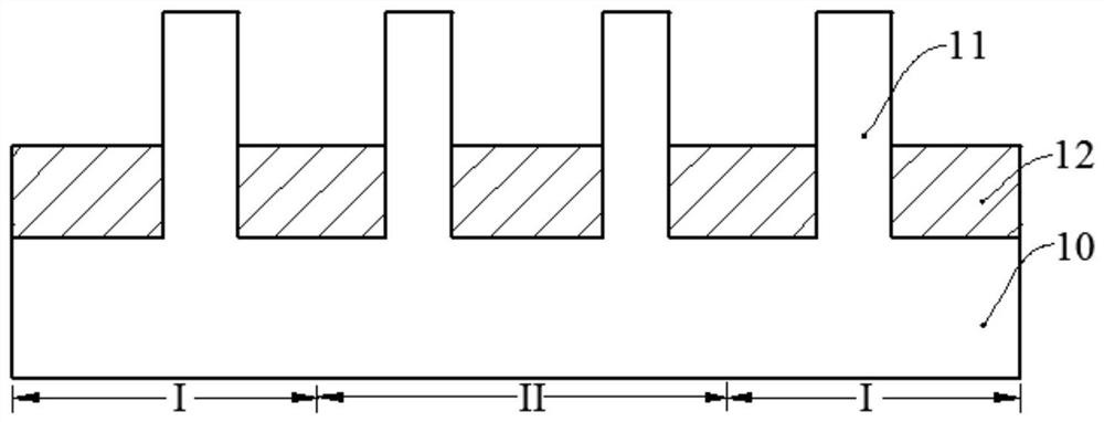
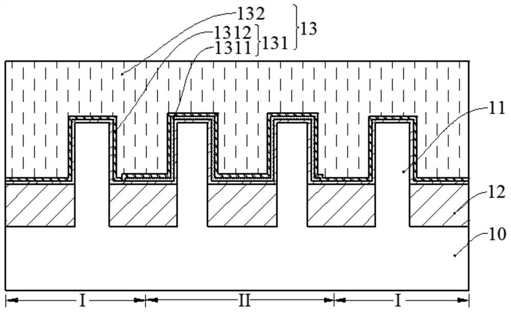
[0016] refer to figure 1 and figure 2 , shows a structural schematic diagram corresponding to each step in a method for forming a semiconductor structure.

[0017] refer to figure 1 , provide a base, the base includes adjacent N-type transistor region I and P-type transistor region II; the base includes a substrate 10 and a fin 11 located on the substrate 10; exposed on the fin 11 An isolation material layer 12 is formed on the substrate 10 , and the isolation material layer 12 covers part of the sidewall of the fin 11 .

[0018] refer to figure 2 , forming a dummy gate structure (not shown in the figure) across the fin 11, and the dummy gate structure covers part of the top wall and part of the sidewall of the fin 11;...


PUM

PropertyMeasurementUnit
widthaaaaaaaaaa

Abstract

The invention discloses a semiconductor structure and a forming method thereof. The forming method comprises the steps of providing a substrate, wherein the substrate comprises an N-type transistor region and a P-type transistor region which are adjacent to each other; forming a work function layer on the substrate, wherein the work function layer comprises a P-type work function layer formed in the P-type transistor region and an N-type work function layer formed in the N-type transistor region; removing the work function layer at the junction of the N-type transistor region and the P-type transistor region to form an opening; and after the opening is formed, forming a gate layer crossing the N-type transistor region and the P-type transistor region on the substrate to form a P-type gatestructure with the remaining P-type work function layer and also form an N-type gate structure with the remaining N-type work function layer. According to the embodiment of the invention, the openingis formed, so that the N-type work function layer or the P-type work function layer is not liable to be located in different types of transistor regions, a process window for forming the work functionlayer is expanded, and the performance of the semiconductor structure is improved.

Description

technical field [0001] Embodiments of the present invention relate to the field of semiconductor manufacturing, and in particular, to a semiconductor structure and a method for forming the same. Background technique [0002] In the current semiconductor industry, integrated circuit products can be mainly divided into three types: logic, memory and analog circuits, among which memory devices account for a considerable proportion of integrated circuit products. With the development of semiconductor technology, storage devices are more widely used, and the storage device and other device regions need to be formed on a chip at the same time to form an embedded semiconductor storage device. For example, to embed the storage device in the central processing unit, it is necessary to make the storage device compatible with the embedded central processing unit platform, and maintain the specifications and corresponding electrical performance of the original storage device. [0003] ...

Claims


Application Information

Patent Timeline
Patent Type & Authority Applications(China)
IPC IPC(8): H01L27/11H01L21/8244H01L21/306H01L21/336
CPCH01L29/66795H01L21/30604H10B99/00H10B10/12
Inventor 张毅俊
Owner SEMICON MFG INT (SHANGHAI) CORP
Why Eureka
Try Eureka