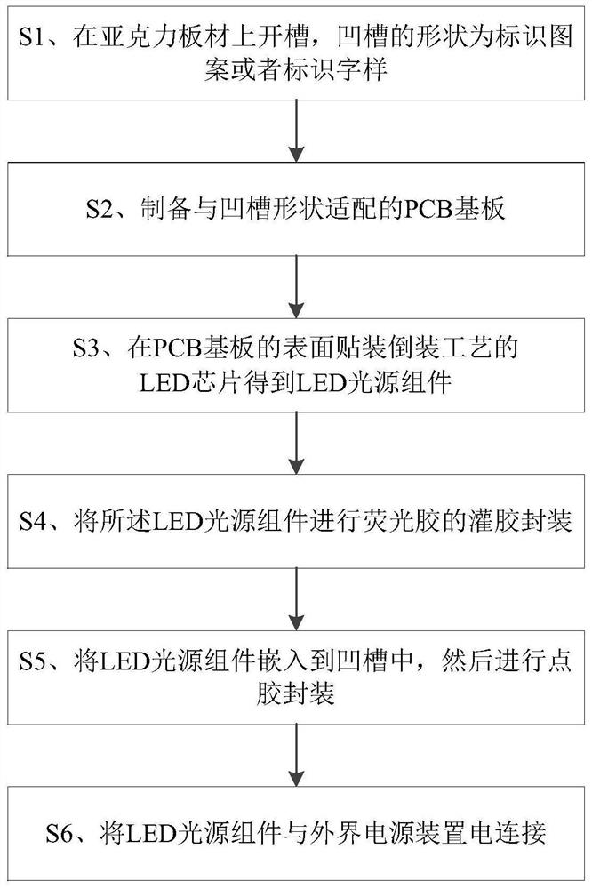
LED signboard preparation process
A technology for preparation process and signage, which is applied to illuminated signs, instruments, display devices, etc., can solve problems such as weak anti-deformation ability, uneven luminescence, and easy-to-damage packaging structure, and achieve enhanced anti-deformation ability and luminous effect Good, guaranteed uniform effect
- Summary
- Abstract
- Description
- Claims
- Application Information
AI Technical Summary
Problems solved by technology
Method used
Image


Examples
Embodiment Construction
[0028] In order to express the present invention more clearly, the present invention will be further described below in conjunction with the accompanying drawings.
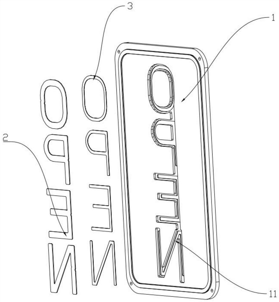
[0029] In our daily life, we can see LED light-emitting signs everywhere, especially at night, when walking in the streets and alleys, we can see the flashing neon lights at a glance, bus stations, subway stations, hospitals, schools, supermarkets, squares, etc. Roadside shops, and other places, are equipped with countless LED light-emitting guide signs. From the point of view of the overall structure, they are all similar. There are a certain number of LED light groups installed inside the LED guide signs. Some of the guide signs themselves are printed cloth, some are PVC, and most of the outer layers are made of acrylic material, that is, transparent plastic. Panel, which can protect the logo and lamp group to a certain extent, prevent man-made damage and rain and fog, and prolong the service life of the logo. ...
PUM
 Abstract
Description
Claims
Application Information