Flip-chip led chip and manufacturing method thereof

A technology of LED chips and manufacturing methods, which is applied in the direction of electrical components, circuits, semiconductor devices, etc., can solve the problems of unclean etching of deep grooves, unsatisfactory etching uniformity, and increased chip manufacturing costs, etc. The effect of quantum efficiency, good current spreading effect, and good lattice matching effect

Active Publication Date: 2018-06-26
HANGZHOU SILAN AZURE
View PDF6 Cites 0 Cited by
  • Summary
  • Abstract
  • Description
  • Claims
  • Application Information

AI Technical Summary

Problems solved by technology

[0004] The high-voltage LED chip structure is generally formed after the epitaxial layer is formed, and the isolation groove is formed by photolithography, and then the isolation groove is filled with insulating material, and finally electrodes are made on each insulated and separated epitaxial layer to form a series structure; although this The structure can improve the luminous brightness of the LED, but the process of forming the isolation groove and filling the insulating material greatly increases the manufacturing cost of the chip. Not only that, but also reduces the reliability of the LED chip to a certain extent. For example, due to the existing etching If the uniformity does not meet the requirements, the deep groove etching is not clean, which will eventually lead to leakage and reduce the breakdown resistance of the LED chip, etc.
[0005] Although the vertical LED chip structure does not need to etch the N-region material, it reduces a part of the production cost of the LED to a certain extent, and is suitable for high-current injection, which can further improve the luminous brightness of the LED chip. However, like the high-voltage chip, the vertical Structured LEDs also need to form isolation grooves, which greatly increases the production cost of LEDs. Not only that, vertical structure chips also need to peel off the growth substrate, which again increases the production cost of LED chips and reduces the cost of LED chips. yield and reliability
[0006] The flip-chip LED chip structure is to flip-chip-weld the front-mounted chip on a substrate with good electrical and thermal conductivity, so that the light-emitting epitaxial layer with relatively concentrated heat generation is closer to the heat-dissipating heat dust, so that most of the heat is exported through the substrate instead of poor heat dissipation. The sapphire growth substrate is exported, which alleviates the heat dissipation problem of the LED chip to a certain extent and improves the reliability of the LED chip; and, when the area of ​​the LED chip is determined, compared with other structures of LED chips, flip-chip The light-emitting area of ​​the LED chip with the structure is larger, so it has more advantages in the face of the challenge of high luminous brightness in the high-end lighting field; however, the flip-chip LED chip structure emits light on the N side, because the refractive index of sapphire is lower than that of nitride The refractive index of gallium, so the light emitted from the epitaxial layer will be reflected on the interface between sapphire and the substrate, resulting in more light not being emitted, especially the patterned substrate currently used in the mainstream LED chip structure has scattering And diffuse reflection, it is easier to cause more light to not be emitted, reducing the light efficiency; but if the patterned substrate technology is not used, the internal quantum efficiency of the LED chip cannot be fully utilized

Method used


Image

  • Flip-chip led chip and manufacturing method thereof
  • Flip-chip led chip and manufacturing method thereof
  • Flip-chip led chip and manufacturing method thereof

Examples


Embodiment 1

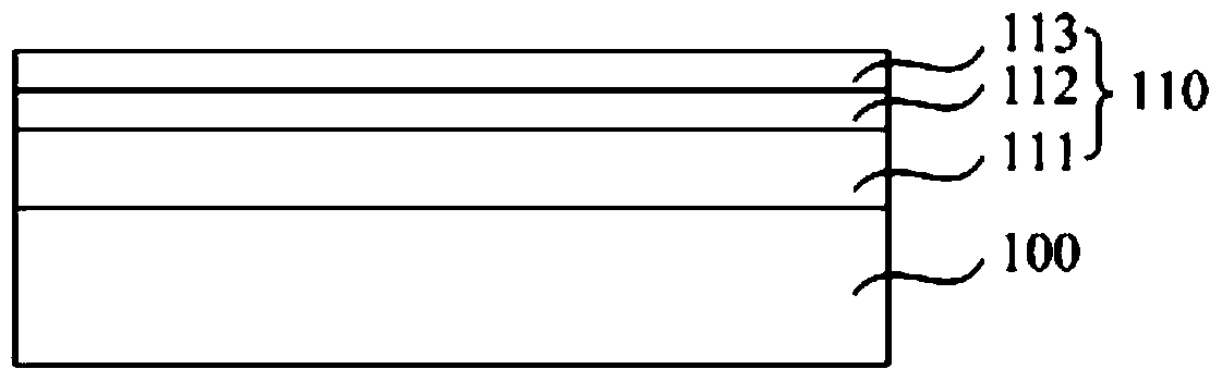
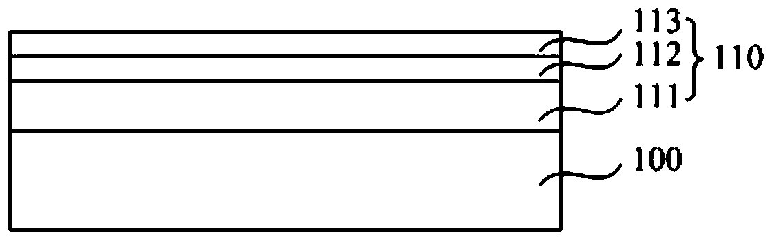
[0063] Such as Figure 1-20 As shown, the flip-chip LED chip includes: a substrate structure 100, an epitaxial layer 110, a contact layer 120, a first connecting electrode 131 and a second connecting electrode 132, an insulating reflective layer 140, a first bonding pad 151 and a second bonding pad Disk 152.

[0064] The substrate structure 100 includes a supporting substrate 101, a lattice matching layer 102, a communication medium layer 103 with periodically arranged columnar structures 103a formed in sequence, and the lattice matching layer 102 is formed on the supporting substrate 101 Above, the communication medium layer 103 is formed on the lattice matching layer 102 and exposes a part of the lattice matching layer 102 .

[0065] The epitaxial layer 110 includes an N-type semiconductor layer 111, an active layer 112, and a P-type semiconductor layer 113 formed in sequence, and the N-type semiconductor layer 111 covers the communication medium layer 103 and the lattice m...

Embodiment 2

[0085] Figure 21 It is a partially enlarged cross-sectional schematic diagram of the substrate structure and the epitaxial layer of the flip-chip LED chip according to the second embodiment of the present invention, Figure 22 It is a partially enlarged top view of the communication medium layer in Embodiment 2 of the present invention.

[0086] Such as Figure 21 with Figure 22 As shown, the difference between this embodiment and Embodiment 1 is that the columnar structure 103a is a columnar protrusion, and the communication medium layer 103 is composed of periodically arranged columnar protrusions, and the crystals are exposed through the gaps between the columnar protrusions. lattice matching layer 102.

[0087] More specifically, the columnar structure 103a is a cylindrical protrusion. Of course, since the supporting substrate 101 is a circular substrate, the columnar structures 103a on the edge of the supporting substrate 101 may be incomplete cylindrical protrusion...

Embodiment 3

[0089] The difference between this embodiment and the first embodiment is that the columnar structure 103a is a polygonal columnar protrusion. Figure 23 It is a partially enlarged top view of the communication medium layer in Embodiment 3 of the present invention. Such as Figure 23 As shown, the columnar structure 103a in this embodiment is a hexagonal columnar protrusion.


PUM


Abstract

The invention provides a flip LED chip and a manufacturing method thereof. The flip LED chip comprises a substrate structure, an epitaxial layer, a contact layer, a first connecting electrode, a second connecting electrode, an insulating reflective layer, a first bonding pad, and a second bonding pad. The substrate structure of the flip LED chip comprises a support substrate, a lattice matching layer and a connecting dielectric layer which are sequentially formed, wherein the connecting dielectric layer is provided with periodically arranged columnar structures, the connecting dielectric layer provided with periodically arranged columnar structures exposes part of the lattice matching layer, and the crystal structure of the lattice matching layer is the same with the crystal structure of an N-type semiconductor layer. The internal quantum efficiency and the external quantum efficiency of the flip LED chip are improved.

Description

technical field [0001] The invention belongs to the field of semiconductor optoelectronic chip manufacturing, in particular to a flip-chip LED chip and a manufacturing method thereof. Background technique [0002] Since the commercialization of GaN-based LEDs in the early 1990s, after more than 20 years of development, its structure has become mature and perfect, and it has been able to meet people's current needs for lighting decoration; but it must completely replace traditional light sources and enter the lighting industry. In the field of lighting, especially in the field of high-end lighting, the improvement of luminous brightness is the never-ending pursuit of scientific researchers in the LED industry. In recent years, the most active technology in improving LED luminance is undoubtedly the patterned substrate technology. The patterned substrate technology not only improves the crystal quality of LED epitaxy by reducing lattice defects (or lattice adaptation), thus gr...

Claims


Application Information

Patent Timeline
Patent Type & Authority Patents(China)
IPC IPC(8): H01L33/22H01L33/46H01L33/62H01L33/02
CPCH01L33/02H01L33/22H01L33/382H01L33/46H01L33/62H01L2933/0008
Inventor 张昊翔丁海生李东昇赵进超黄捷陈善麟江忠永
Owner HANGZHOU SILAN AZURE
Why Eureka
Try Eureka