LED integrated light source manufacturing process and LED integrated light source

A manufacturing process and light source technology, applied in electrical components, pretreated surfaces, electrical solid devices, etc., can solve problems such as affecting the luminous effect of LED integrated light sources, reducing excitation efficiency, and low brightness, reducing the risk of cracking. Improve service life and ensure uniformity

Inactive Publication Date: 2020-12-11
GUANGDONG GMA OPTOELECTRONICS TECH +3
View PDF21 Cites 0 Cited by
  • Summary
  • Abstract
  • Description
  • Claims
  • Application Information

AI Technical Summary

Problems solved by technology

Since the content of fluorescent glue in the powder-glue mixture is much greater than that of phosphor powder, it is easy to cause problems such as low phosphor content and low brightness of light after being excited; at the same time, due to the different particle sizes and densities of phosphor powder, there are The phosphor concentration of the powder-glue mixture is not uniform, and then the excitation efficiency decreases at the position where the phosphor concentration is low, especially at the edge of the chip to form a dark area, which affects the luminous effect of the LED integrated light source; in addition, due to the droplet The amount of powder-glue mixture is large. When the LED integrated light source is driven by high-power products or used for a long time, when the fluorescent layer heats up locally, it is easy to crack the glue, leading to failure and seriously affecting the use.

Method used


Image

  • LED integrated light source manufacturing process and LED integrated light source
  • LED integrated light source manufacturing process and LED integrated light source
  • LED integrated light source manufacturing process and LED integrated light source

Examples


Embodiment Construction

[0040] In order to make the technical problems solved by the present invention, the technical solutions adopted and the technical effects achieved clearer, the technical solutions of the embodiments of the present invention will be further described in detail below in conjunction with the accompanying drawings. Obviously, the described embodiments are only the technical solutions of the present invention. Some, but not all, embodiments. Based on the embodiments of the present invention, all other embodiments obtained by those skilled in the art without creative efforts fall within the protection scope of the present invention.

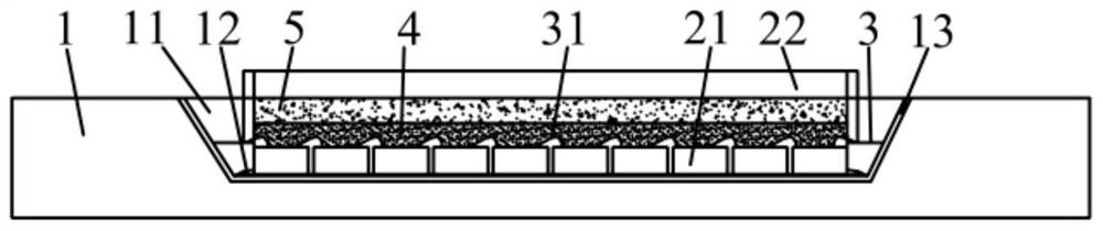
[0041] like Figure 1-Figure 3 As shown, this embodiment provides an LED integrated light source manufacturing process and an LED integrated light source. The steps of the LED integrated light source manufacturing process include: S10, bonding a plurality of chips 21 to the counterbore 11 of the substrate 1 through an adhesive 12 Inside, bake to form ...


PUM

PropertyMeasurementUnit
Thicknessaaaaaaaaaa

Abstract

The invention relates to the technical field of LED integrated light sources, and discloses an LED integrated light source manufacturing process and an LED integrated light source. The manufacturing process of the LED integrated light source comprises the following steps: S10, adhering a plurality of chips into counter bores of a substrate through an adhesive, and baking to form a chip layer; S20,conducting the plurality of chips, and reserving lead layers conducted with the chips; S30, placing an edge shielding frame, mixed fluorescent powder, fluorescent glue and a diluent on the peripheryof the chip layer, spray-covering the chip layer, taking down the edge shielding frame, baking to form a fluorescent layer, and placing the chip layer in the fluorescent layer; and S40, dispensing a packaging adhesive on the fluorescent layer, baking to form a packaging layer, and placing the chip layer in the packaging layer. According to the invention, by adding the diluent, the viscosity of thepowder glue mixed solution is reduced, the content of fluorescent powder is increased, and the brightness of light generated after excitation is ensured to be higher; and the spraying mode enables the excitation efficiency of each position of the chip to be the same, guarantees the light-emitting uniformity, reduces the risk of glue cracking, and prolongs the service life of the LED integrated light source.

Description

technical field [0001] The invention relates to the technical field of LED integrated light source, in particular to a manufacturing process of LED integrated light source and the LED integrated light source. Background technique [0002] LED integrated light source has the advantages of energy saving, environmental protection, and long life, and is widely used in occasions that require various lighting. [0003] At present, LED integrated light sources have different packaging forms and structures in the field of packaging. The traditional packaging process is mostly dispensing process, that is, mixing phosphor powder and fluorescent glue, dripping it on the chip, and then baking and curing to form a fluorescent layer. Since the content of fluorescent glue in the powder-glue mixture is much greater than that of phosphor powder, it is easy to cause problems such as low phosphor content and low brightness of light after being excited; at the same time, due to the different pa...

Claims


Application Information

Patent Timeline
IPC IPC(8): H01L33/50H01L25/075B05D3/02B05D1/38
CPCH01L33/501H01L33/505H01L25/0753B05D1/38B05D3/0254H01L2933/0041
Inventor 戢利进廖勇军李文庭张诺寒
Owner GUANGDONG GMA OPTOELECTRONICS TECH
Why Eureka
Try Eureka