A method for judging optical catastrophe type of semiconductor laser chip

A technology of optical catastrophe and laser, which is applied in semiconductor lasers, lasers, laser components, etc., can solve the problems of low production efficiency, high judgment cost, and long judgment time, and achieve the effects of low cost, improved efficiency, and improved reliability

Active Publication Date: 2021-06-15
灵素医疗科技(陕西)有限公司
View PDF14 Cites 0 Cited by
  • Summary
  • Abstract
  • Description
  • Claims
  • Application Information

AI Technical Summary

Problems solved by technology

[0006] The purpose of the present invention is to solve the problems of high judgment cost, long judgment time and low production efficiency of existing semiconductor laser chips COBD and COMD, and to provide a method for judging the optical catastrophe type of semiconductor laser chips

Method used


Image

  • A method for judging optical catastrophe type of semiconductor laser chip
  • A method for judging optical catastrophe type of semiconductor laser chip
  • A method for judging optical catastrophe type of semiconductor laser chip

Examples


Embodiment 1

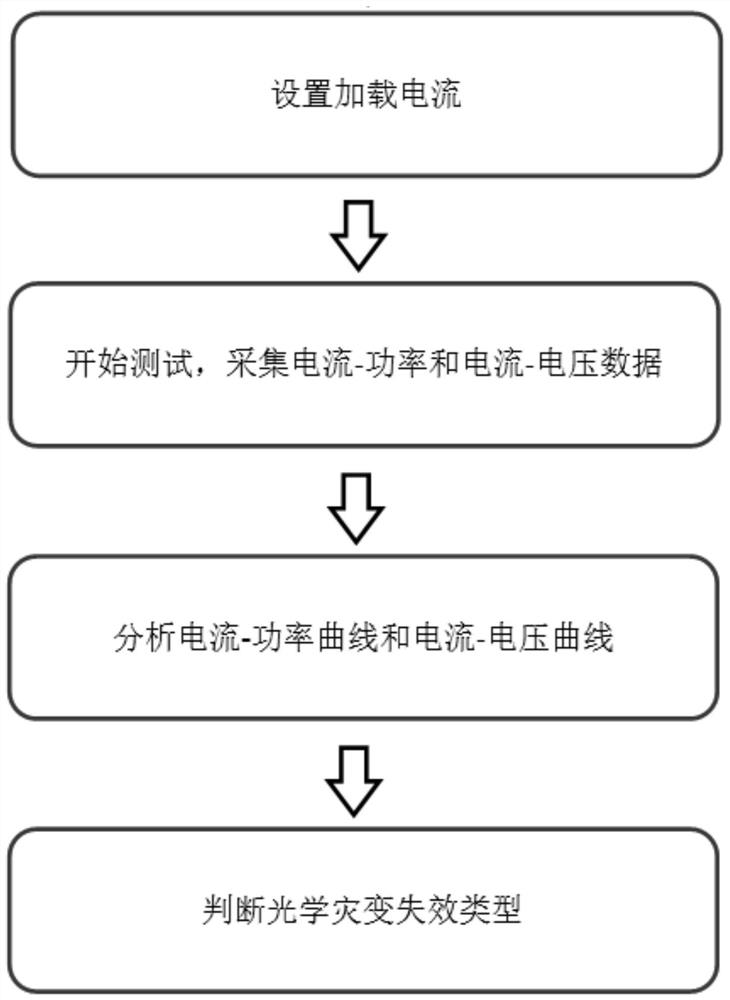
[0049] The present invention judges the method for semiconductor laser chip (bare chip) optical catastrophe type to comprise the following steps:

[0050] Step 1. Set the step size of the current rise and the maximum current (adjust accordingly according to the product type);

[0051] Step 2. Place the coated bare bar chip on the bar test bench, with the P side up (positive electrode), and the N side metal of the bar chip contacts the copper strip of the test bench, and the copper strip will be electrically connected to the negative electrode; Adjust the two probes of the test bench, apply current to one of the probes, and make contact with the P side of the bare bar chip, and the other probe collects the voltage of the bar chip;

[0052] Step 3, turn on the power supply, collect the current-power curve of the test chip, and collect the current-voltage curve at the same time;

[0053] Step 4, analyze the current-power curve and current-voltage curve, such as figure 2 As sho...

Embodiment 2

[0055] The present invention judges the method for semiconductor laser chip (COS chip) optical catastrophe type to comprise the following steps:

[0056] Step 1. Set the step size of the current rise and the maximum current (adjust accordingly according to the product type);

[0057] Step 2. Install the packaged COS chip on the COS test fixture, and then install the test fixture on the COS test platform; connect the positive and negative electrodes to the COS test fixture, where the positive and negative electrodes are connected to the data acquisition card, which can collect current and voltage Data and power data are collected by an integrating sphere;

[0058] Step 3, turn on the power supply, collect the current-power curve of the test chip, and collect the current-voltage curve at the same time;

[0059] Step 4, analyze the current-power curve and current-voltage curve, such as image 3 As shown, the failure type is judged according to the change of the current-voltage ...

Embodiment 3

[0061] The present invention judges the method for the optical catastrophe type of semiconductor laser chip (COS chip aging) to comprise the following steps:

[0062] Step 1. Set the aging current;

[0063] Step 2. Install the packaged COS chip on the COS aging fixture, and then install the aging fixture on the COS aging cabinet; add the aging current required by the product to the COS aging cabinet, where the positive and negative poles of the COS aging fixture are connected to the data acquisition card, which can Collect current and voltage data, and power data is collected by an integrating sphere;

[0064] Step 3, monitoring the power value change trend and the voltage value change trend of COS device aging;

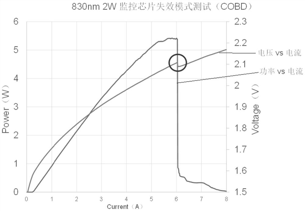
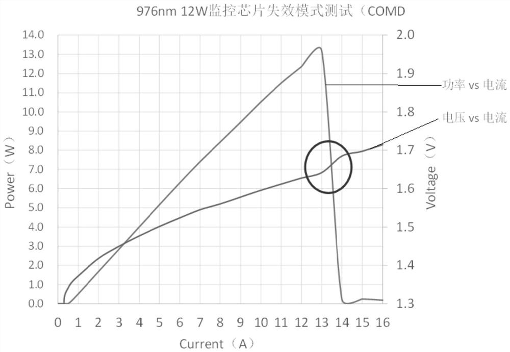
[0065] Step 4. Analyze the power trend curve and voltage value trend curve of COS device aging. When the monitored power value suddenly drops and the voltage value drops, it is judged that the failure of the COS device is COBD; if the power value suddenly drops, the...


PUM


Abstract

The invention provides a method for judging the optical catastrophe type of a semiconductor laser chip, which solves the problems of high judgment cost, long judgment time and low production efficiency of existing semiconductor laser chips COBD and COMD. The method includes: Step 1, setting the loading current; Step 2, loading the loading current on the semiconductor laser chip; Step 3, collecting the current-power curve and current-voltage curve of the semiconductor laser chip; Step 4, if the current-power curve If the current-voltage curve suddenly drops and the current-voltage curve suddenly rises, it is judged that the optical catastrophe of the chip is COMD; if the current-power curve suddenly drops and the current-voltage curve suddenly drops, it is judged that the optical catastrophe of the chip is COBD. The method of the present invention does not require professional equipment, and only needs to collect the current, power value and voltage value in the test process to judge COBD and COMD. The detection equipment is simple and the cost is low, and only ordinary technicians can realize the judgment of failure .

Description

technical field [0001] The invention belongs to the field of semiconductor laser failure analysis, in particular to a method for judging the type of optical catastrophe of a semiconductor laser chip. Background technique [0002] As an indirect or direct light source, semiconductor lasers are increasingly used in laser optical fiber communications, industrial shipbuilding, automobile manufacturing, laser engraving, laser marking, laser cutting, printing rolls, metal and non-metal drilling / cutting / welding and other fields. At the same time, with the development of intelligence and miniaturization, semiconductor lasers have gradually become the main pump source of fiber lasers. [0003] If the semiconductor laser chip is to exert the performance of the epitaxial design, the epitaxial material growth and chip manufacturing (cavity surface coating) are particularly important. Defects or inhomogeneities generated during the growth of epitaxial materials will affect the reliabili...

Claims


Application Information

Patent Timeline
Patent Type & Authority Patents(China)
IPC IPC(8): H01S5/00
CPCH01S5/0014H01S5/0021H01S5/0035H01S5/0042
Inventor 任占强李波李青民王宝超李喜荣仇伯仓
Owner 灵素医疗科技(陕西)有限公司
Why Eureka
Try Eureka