Super-junction VDMOS

A conductive type, semiconductor technology, applied in the direction of electrical components, circuits, semiconductor devices, etc., can solve problems such as broadband, electromagnetic pollution, etc., to achieve the effect of improving EMI, increasing capacitance value, and alleviating electromagnetic interference

Active Publication Date: 2020-11-20
UNIV OF ELECTRONIC SCI & TECH OF CHINA
View PDF6 Cites 0 Cited by
  • Summary
  • Abstract
  • Description
  • Claims
  • Application Information

AI Technical Summary

Problems solved by technology

The electromagnetic interference generated by the power VDMOS itself has a strong amplitude and a wide frequency band. These interferences will cause serious electromagnetic pollution to the su

Method used


Image

  • Super-junction VDMOS
  • Super-junction VDMOS
  • Super-junction VDMOS

Examples


Embodiment 1

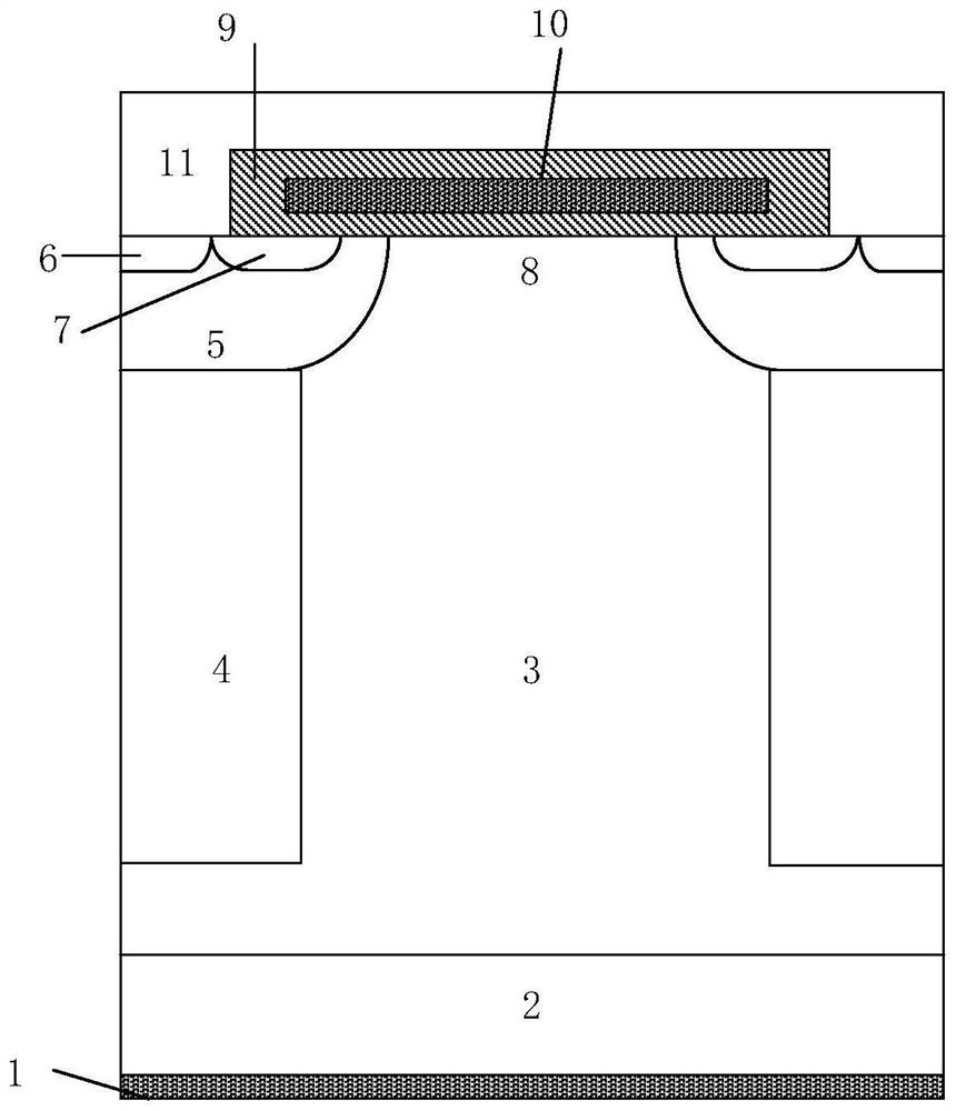
[0021] Such as image 3 As shown, this example includes a metallized drain 1, a heavily doped first conductivity type semiconductor substrate 2 on the metallized drain 1, a lightly doped first conductivity type semiconductor substrate 2 on the first conductivity type conductivity type semiconductor region 3; the lightly doped first conductivity type semiconductor region 3 has a second conductivity type semiconductor body region 5 on both sides of the top; the second conductivity type semiconductor body region 5 is lightly doped with the first conductivity type Miscellaneous JFET region 8; the second conductivity type semiconductor body region 5 has a second conductivity type semiconductor heavily doped contact region 6 and a first conductivity type semiconductor source region 7, the first conductivity type semiconductor source region 7 and the first conductivity type semiconductor The second conductivity type semiconductor body region 5 between the lightly doped JFET regions 8...

Embodiment 2

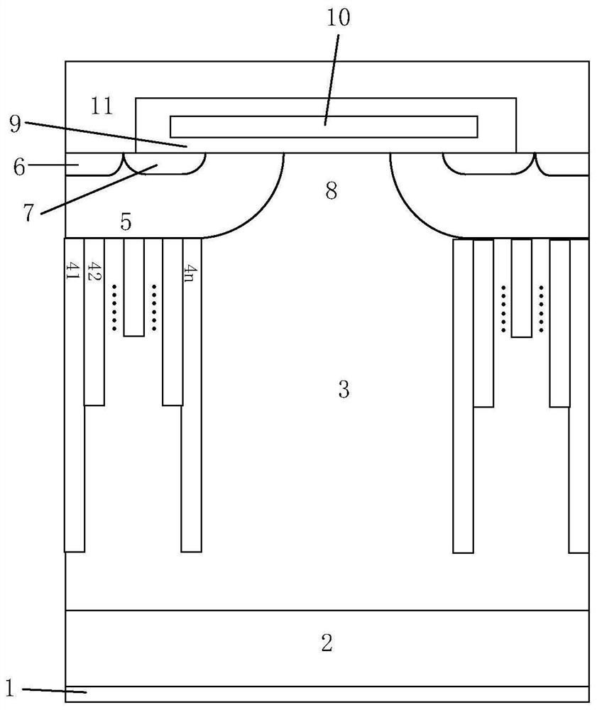
[0026] Such as Figure 4 As shown, on the basis of Embodiment 1, the semiconductor region 12 of the first conductivity type is added under the semiconductor pillars 42 of the second conductivity type. The upper surface of the first conductivity type semiconductor region 12 is in direct contact with the second conductivity type semiconductor pillar 42 , and the lower surface is flush with the second conductivity type semiconductor pillar 41 , 43 . The doping concentration of the first conductivity type semiconductor region 12 is higher than that of the lightly doped first conductivity type semiconductor region 3 . It is also characterized in that the total amount of impurities in the semiconductor columns 41, 42, 43 of the second conductivity type and the total amount of impurities in the lightly doped semiconductor region 3 of the first conductivity type and the semiconductor region 12 of the first conductivity type satisfy the charge balance.

Embodiment 3

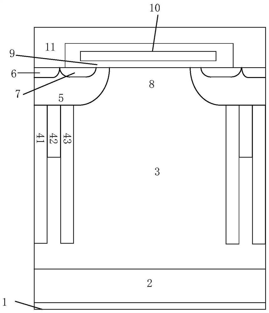
[0028] In this example, on the basis of Embodiment 1, the doping concentration of the second conductivity type semiconductor pillars 42 located in the middle is lower than the doping concentrations of the second conductivity type semiconductor pillars 41 and 43 located on both sides.


PUM


Abstract

The invention belongs to the technical field of power semiconductors, and relates to a super-junction VDMOS. According to the super-junction VDMOS capable of improving EMI provided by the invention, asecond conductive type semiconductor voltage-withstanding columns with different lengths are introduced into a drift region, so that the longitudinal broadening of a depletion layer between the gateand the drain of a super-junction device is relieved, and the Cgd capacitance value is increased when Vds is smaller, so that a Cgd-Vds curve is flatter. Effective alleviation of voltage and current overshoot is realized. Therefore, the problem of electromagnetic interference of the device can be relieved on the basis of ensuring the original basic electrical properties of the super-junction VDMOS.

Description

technical field [0001] The invention belongs to the technical field of power semiconductors and relates to a super junction VDMOS. Background technique [0002] The power super-junction VDMOS structure uses alternating P-columns and N-columns to replace the N-drift region of traditional power devices, thereby effectively reducing the on-resistance and obtaining lower on-state power consumption. Due to its unique high input impedance, low driving power, high switching speed, superior frequency characteristics, and good thermal stability, it is widely used in various fields such as switching power supplies, automotive electronics, and motor drives. Traditional superjunction VDMOS structures such as figure 1 shown. [0003] The typical application environment of power VDMOS devices is switching power supply. In order to meet the miniaturization requirements of switching power supply, its switching frequency and power density are constantly increasing. Modularization and funct...

Claims


Application Information

Patent Timeline
IPC IPC(8): H01L29/06H01L29/78
CPCH01L29/0634H01L29/7811
Inventor 任敏郭乔蓝瑶瑶李吕强高巍李泽宏张金平张波
Owner UNIV OF ELECTRONIC SCI & TECH OF CHINA
Why Eureka
Try Eureka