Supercharge Your Innovation With Domain-Expert AI Agents!

Heating device and bonding device

A heating device and heating element technology, which is applied in the fields of electrical components, semiconductor/solid-state device manufacturing, circuits, etc., can solve the problems of low heating efficiency, achieve weight reduction, good thermal conductivity, and improve heating efficiency

Active Publication Date: 2020-12-04
SHANGHAI MICRO ELECTRONICS EQUIP (GRP) CO LTD
View PDF4 Cites 0 Cited by
  • Summary
  • Abstract
  • Description
  • Claims
  • Application Information

AI Technical Summary

Problems solved by technology

[0004] The object of the present invention is to provide a heating device and a bonding device to solve the problem of low heating efficiency of existing heating devices and bonding devices

Method used


Image

  • Heating device and bonding device
  • Heating device and bonding device
  • Heating device and bonding device

Examples


Embodiment 1

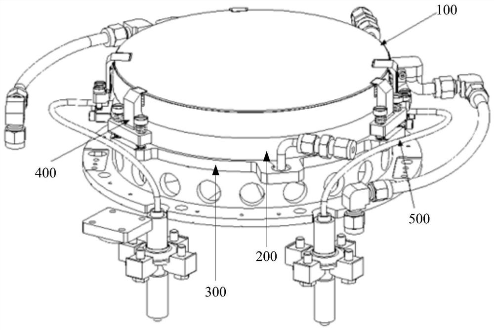
[0068] This embodiment provides a heating device. refer to figure 1 and figure 2 , figure 1 is a schematic structural view of the heating device in Embodiment 1 of the present invention, figure 2 It is a schematic cross-sectional view of the heating device in Embodiment 1 of the present invention, and the heating device includes a heating unit 100 , a cooling unit 200 , a base 300 , a fixing unit 400 and a wire unit 500 .

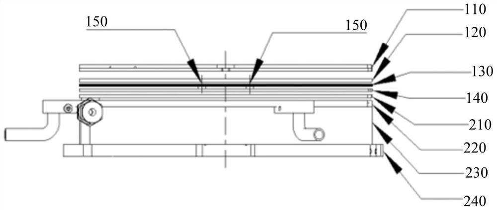
[0069] refer to figure 2 , the heating unit 100 includes a surface layer 110 , an upper supporting layer 120 , a heating element 130 , a lower supporting layer 140 and at least one positioning pin 150 stacked in sequence.

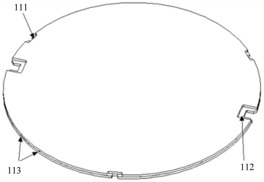
[0070] refer to image 3 , image 3 It is a schematic structural diagram of the surface layer 110 in Embodiment 1 of the present invention. The surface layer 110 is located on the uppermost layer and can be in direct contact with the workpiece to be heated, so as to make the workpiece to be heated uniformly heated. The surface ...

Embodiment 2

[0111] This embodiment provides a heating device. The difference between the heating device in this embodiment and the heating device in Embodiment 1 is that the heating device in this embodiment includes a heating unit 100, a cooling unit 200, a base 300, a wire unit 500 and a fixing unit 400, but the The cooling unit 200 does not include the cooling member 220 . The lower supporting layer 140 in the heating unit 100 is arranged on the heat conduction layer 210 in the cooling unit 200, the heat conduction layer 210 is arranged on the heat insulation layer 230, and the heat insulation layer 230 is arranged on the bottom layer 240 superior. The fixing unit 400 is used to fix the heating unit 100 and the cooling unit 200 on the base 300 .

[0112] In other embodiments, the heating device does not include the cooling unit 200, the lower support layer 140 in the heating unit 100 is arranged on the base 300, and the fixing unit 400 is used to fix the heating unit 100 On the base...

Embodiment 3

[0114] This embodiment provides a heating device. The difference between the heating device in this embodiment and the heating device in Embodiment 1 is that the heating device in this embodiment further includes a pressing plate, and the pressing plate is arranged on the side of the surface layer 110 away from the upper supporting layer 120 , the press plate can directly contact the surface of the wafer and apply pressure to the wafer for bonding.

[0115] The material of the pressing plate is preferably silicon carbide.


PUM


Abstract

The invention provides a heating device and a bonding device. The heating device is used for heating a workpiece, and comprises a base, and a surface layer, an upper support layer, a heating piece anda lower support layer which are stacked in sequence, wherein the lower support layer is arranged close to the base, the surface layer, the upper support layer, the heating piece and the lower supportlayer are connected with the base, the surface layer is used for uniformly heating a workpiece, the heating piece is used for generating heat, and the upper support layer and the lower support layerare used for supporting the heating piece. According to the invention, heat can be generated through the sheet-shaped heating piece and transmitted to a workpiece through the upper support layer and the surface layer, so that the thickness of the heating device is reduced, and the weight of the heating device is reduced so as to improve the heating efficiency and increase the temperature conduction rate.

Description

technical field [0001] The invention relates to the technical field of semiconductors, in particular to a heating device and a bonding device. Background technique [0002] The technology that two wafers with flat and clean surfaces are bonded to each other through chemical bonds on the surface under certain conditions is called wafer bonding technology. Free combination of different materials is widely used in microelectronic circuits, sensors, power devices, micromachining, optoelectronic devices, silicon-on-insulator (SOI) and other fields. At present, wafer bonding technology can be used to make many important optoelectronic devices. [0003] The wafer bonding process is generally in a vacuum environment, under the condition of applying a predetermined pressure to the materials to be bonded, such as silicon wafers and glass substrates, heating these bonding materials to a predetermined temperature and continuing for a period of time until Complete wafer bonding. In th...

Claims


Application Information

Patent Timeline
Patent Type & Authority Applications(China)
IPC IPC(8): H01L21/67
CPCH01L21/67109H01L21/67092
Inventor 赵滨李秀华朱鸷
Owner SHANGHAI MICRO ELECTRONICS EQUIP (GRP) CO LTD
Features
  • R&D
  • Intellectual Property
  • Life Sciences
  • Materials
  • Tech Scout
  • Unparalleled Data Quality
  • Higher Quality Content
  • 60% Fewer Hallucinations
Learn More