
Semiconductor silicon wafer patch based on thermal winding technology

A semiconductor and chip technology, which is applied in the field of semiconductor silicon chip patch based on heat entanglement technology, can solve the problem of semiconductor silicon wafer and chip bulge, the occurrence of bubbles between chip and semiconductor silicon chip, and the problem of chip and semiconductor silicon chip. Insufficient bonding and other problems to achieve the effect of improving the connection strength

Pending Publication Date: 2020-12-04
孙福志
View PDF0 Cites 3 Cited by
  • Summary
  • Abstract
  • Description
  • Claims
  • Application Information

AI Technical Summary

Problems solved by technology

[0004] In the prior art, during the process of bonding semiconductor silicon wafers, air bubbles are likely to appear between the patch and the semiconductor silicon wafer, thus making the bonding between the patch and the semiconductor silicon wafer weak, and at the same time, during use, Due to the increase in temperature, it may cause a bulge between the semiconductor silicon wafer and the patch

Method used


Image

  • Semiconductor silicon wafer patch based on thermal winding technology
  • Semiconductor silicon wafer patch based on thermal winding technology
  • Semiconductor silicon wafer patch based on thermal winding technology

Examples


Embodiment 1

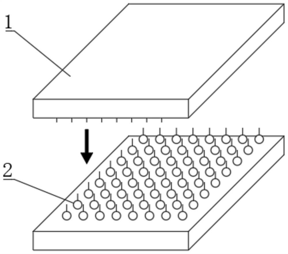
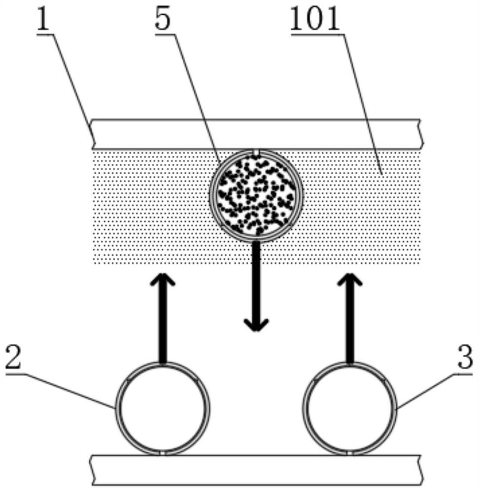
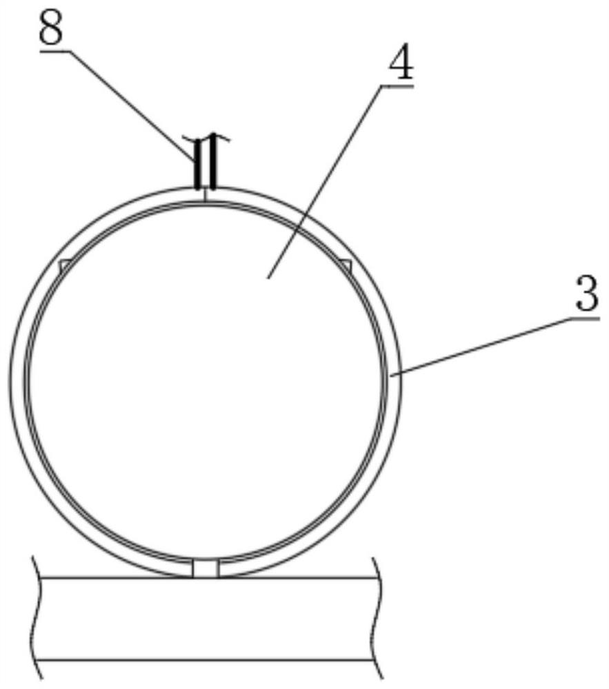
[0043] see Figure 1-8 , a semiconductor silicon chip patch based on thermal winding technology, including a patch body 1 and a plurality of evenly distributed scattered hook balls 2, the scattered hook balls 2 are usually evenly distributed and bonded to the semiconductor silicon wafer during actual use. On the sheet surface, the scattered hook balls 2 include a first outer encapsulation layer 3, the inner bottom of the first outer encapsulation layer 3 is fixedly connected with the main magnetic ball 4, and the bottom end of the patch main body 1 is fixedly connected with the second outer encapsulation layer 5, the second The inner top of the outer encapsulation layer 5 is fixedly connected with a reaction mill ball 6, the first outer encapsulation layer 3 and the second outer encapsulation layer 5 are composed of a plurality of evenly distributed fan-shaped capsules 7, and the upper end of the first outer encapsulation layer 3 is fixedly connected There are a plurality of e...


PUM


Abstract

The invention discloses a semiconductor silicon wafer patch based on a thermal winding technology, and belongs to the technical field of semiconductor silicon wafers. A first outer envelope layer canbe promoted to be peeled off from the outer side of a main magnetic ball by virtue of a counter-acting force, and meanwhile, a second outer envelope layer can be peeled off from the outer side of theexposed main magnetic ball under the attraction action. Reaction grinding balls in the second outer envelope layer are promoted to be exposed, the reaction grinding balls are promoted to react with air to release a large amount of heat, on one hand, air between the semiconductor silicon wafer and the patch can be exhausted by means of heat generated in the reaction process, and therefore the air amount in the semiconductor silicon wafer and the patch is reduced; on the other hand, by means of the attraction effect between ferroferric oxide powder generated after the reaction and the second outer envelop layer and the attraction effect of the second outer envelop layer on a lower inverted hook, an upper inverted hook and the lower inverted hook can be simulated into bristles and soft bristles of hook-and-loop fasteners; therefore, the connection strength between the semiconductor silicon wafer and the patch is improved.

Description

technical field [0001] The invention relates to the technical field of semiconductor silicon wafers, and more specifically, relates to a semiconductor silicon wafer patch based on thermal winding technology. Background technique [0002] Semiconductors refer to materials whose conductivity is between conductors and insulators at room temperature. Semiconductors are used in integrated circuits, consumer electronics, communication systems, photovoltaic power generation, lighting, high-power power conversion and other fields. For example, diodes are devices made of semiconductors. , no matter from the perspective of technology or economic development, the importance of semiconductors is very huge. The core units of most electronic products, such as computers, mobile phones or digital recorders, are closely related to semiconductors. , common semiconductor materials include silicon, germanium, gallium arsenide, etc., and silicon is the most influential one in the application of ...

Claims


Application Information

Patent Timeline
Patent Type & Authority Applications(China)
IPC IPC(8): H01L21/67H01L21/683
CPCH01L21/67144H01L21/6836H01L2221/68381
Inventor 孙福志
Owner 孙福志
Learn More