

Splicing coating method for semiconductor part
A technology for semiconductors and components, applied in the field of splicing and coating of semiconductor components, can solve the problems that are not involved, have not been improved, and the target cannot be fully coated, and achieve the effect of ensuring strength performance and avoiding changes in grains.
- Summary
- Abstract
- Description
- Claims
- Application Information
AI Technical Summary
Problems solved by technology
Method used
Image

Examples
Embodiment 1
[0069] This embodiment provides a splicing coating method for semiconductor components, the method comprising the following steps:
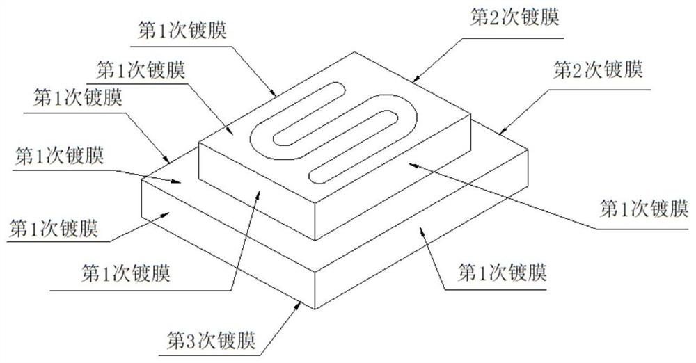
[0070] (1) The semiconductor part is first cleaned, the semiconductor part is an aluminum part, and its shape is a cube, then the surface of the semiconductor part in contact with the clamp in the coating equipment is shielded by a metal tin protective film, and the protective film is passed through The silicone adhesive is attached to the surface of the semiconductor component, and then dried at 50°C;
[0071] (2) Coating the semiconductor component after step (1) in the magnetron sputtering coating equipment, controlling the coating temperature to be 70°C, and the coating power is 60kW, to complete the coating on the non-shielded surface, and the thickness of the formed coating is 5 μm, Coating material is titanium;
[0072] (3) metal tin protective film is attached to the surface of coating film in step (2), described protective film is attac...
Embodiment 2
[0075] This embodiment provides a splicing coating method for semiconductor components, the method comprising the following steps:
[0076] (1) The semiconductor part is first cleaned, the semiconductor part is a stainless steel part, and its shape is a cube, then the surface of the semiconductor part in contact with the clamp in the coating equipment is shielded by a metal aluminum protective film, and the protective film passes through The acrylic resin adhesive is attached to the surface of the semiconductor component, and then dried at 60°C;
[0077] (2) Coating the semiconductor component after step (1) in the magnetron sputtering coating equipment, controlling the coating temperature to be 80°C, and the coating power is 45kW, to complete the coating on the non-shielded surface, and the thickness of the formed coating is 6 μm, The coating material is nickel;
[0078] (3) attach metal aluminum protective film to the surface of coating film in step (2), described protectiv...
Embodiment 3
[0081] This embodiment provides a splicing coating method for semiconductor components, the method comprising the following steps:
[0082] (1) The semiconductor part is cleaned first, and the semiconductor part is made of titanium, and its shape is disc-shaped; The film is attached to the surface of the semiconductor component through a polytetrafluoroethylene resin adhesive, and then dried at 40°C;
[0083] (2) Coating the semiconductor component after step (1) in the magnetron sputtering coating equipment, controlling the coating temperature to be 60°C, and the coating power is 90kW, to complete the coating on the non-shielded surface, and the thickness of the formed coating is 3 μm, The coating material is nickel;
[0084] (3) the metal tin protective film is attached to the surface of the coating film in the step (2), the protective film is attached to the coating film surface by a polytetrafluoroethylene resin binder, and the protective film is modified after being form...
PUM
| Property | Measurement | Unit |
|---|---|---|
| thickness | aaaaa | aaaaa |
Abstract
Description
Claims
Application Information