
Athermal arrayed waveguide grating

A technology of arrayed waveguide and waveguide grating, which is applied in the direction of optical waveguide light guide, optics, light guide, etc., can solve the problems of incapable of mass production and incompatibility with CMOS process, and realize the temperature insensitivity of central wavelength, good process compatibility, good The effect of temperature stability

Active Publication Date: 2022-07-05
UNITED MICROELECTRONICS CENT CO LTD
View PDF6 Cites 0 Cited by
  • Summary
  • Abstract
  • Description
  • Claims
  • Application Information

AI Technical Summary

Problems solved by technology

However, although these two methods have good temperature stability control effects, for integrated optical processes such as SOI and SIN, these two methods are not compatible with traditional CMOS processes, and cannot be mass-produced quickly.

Method used


Image

  • Athermal arrayed waveguide grating
  • Athermal arrayed waveguide grating
  • Athermal arrayed waveguide grating

Examples


Embodiment Construction

[0041] The embodiments of the present invention are described below through specific specific examples, and those skilled in the art can easily understand other advantages and effects of the present invention from the contents disclosed in this specification. The present invention can also be implemented or applied through other different specific embodiments, and various details in this specification can also be modified or changed based on different viewpoints and applications without departing from the spirit of the present invention.

[0042] When describing the embodiments of the present invention in detail, for the convenience of explanation, the cross-sectional views showing the device structure will not be partially enlarged according to the general scale, and the schematic diagrams are only examples, which should not limit the protection scope of the present invention. In addition, the three-dimensional spatial dimensions of length, width and depth should be included i...


PUM

PropertyMeasurementUnit
widthaaaaaaaaaa

Abstract

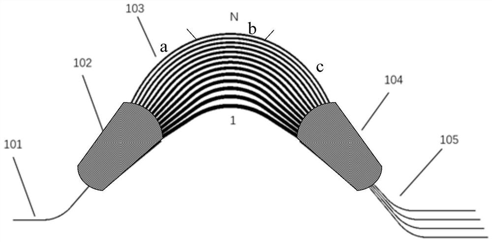
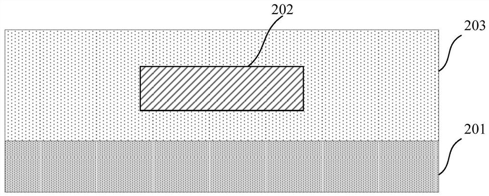
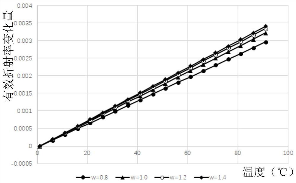
The present invention provides an athermal arrayed waveguide grating. In the arrayed waveguide, adjacent arrayed waveguides have different waveguide lengths, and corresponding adjacent arrayed waveguides have different waveguide widths, and the waveguide widths of the arrayed waveguides vary with the length of the arrayed waveguides. The length of the waveguide decreases with the increase of the waveguide length. By changing the waveguide width of the arrayed waveguide, the athermalization of the arrayed waveguide grating can be realized. It can maintain good temperature stability without external power supply. It can reduce the system maintenance cost; the design and process are simple, no post-processing process is required, it can be adapted to mass production and commercialization, and the performance is stable; it has good process compatibility, and can be processed by standard CMOS; multiplexing. The athermal arrayed waveguide grating of the present invention can realize the temperature insensitivity of the center wavelength under the premise of ensuring that the optical path difference of adjacent arrayed waveguides is fixed as a whole.

Description

technical field [0001] The invention belongs to the field of optical communication and integrated optics, and relates to an athermal arrayed waveguide grating. Background technique [0002] With the development of 5G Internet, people's demand for data transmission is increasing. Optical communication has become the main method of network information transmission at present, but the demand for data transmission has grown very rapidly in recent years. In order to increase the network transmission bandwidth and reduce the cost of network data transmission, the wavelength division multiplexing system has become the main solution to increase the network bandwidth. [0003] At present, there are two main methods for realizing wavelength division multiplexing: one is a wavelength division multiplexing device made based on a geometrical optical lens system, and the other is a wavelength division multiplexing device made based on integrated optics. Among them, the wavelength divisi...

Claims


Application Information

Patent Timeline
Patent Type & Authority Patents(China)
IPC IPC(8): G02B6/12
CPCG02B6/12026
Inventor 杨忠华李智慧何来胜梁宇鑫崔乃迪
Owner UNITED MICROELECTRONICS CENT CO LTD
Learn More