Ultraviolet photodiode based on NiFe2O4/Ga2O3 and preparation method of ultraviolet photodiode

A technology of diodes and ultraviolet light, which is applied in the direction of circuits, electrical components, semiconductor devices, etc., can solve problems such as the inability to prepare Ga and lack of materials, and achieve high critical breakdown electric field strength, excellent detection performance, and improved reliability.

Active Publication Date: 2020-12-11
西安千月电子科技有限公司
View PDF5 Cites 2 Cited by
  • Summary
  • Abstract
  • Description
  • Claims
  • Application Information

AI Technical Summary

Problems solved by technology

[0004] The purpose of this invention is to provide a kind of NiFe-based 2 o 4 / Ga 2 o 3 The UV photodiode solves the problem of p-type Ga in the prior art 2 o 3 The lack of materials prevents the preparation of Ga 2 o 3 Problems with base pn junction UV photodiodes

Method used


Image

  • Ultraviolet photodiode based on NiFe2O4/Ga2O3 and preparation method of ultraviolet photodiode
  • Ultraviolet photodiode based on NiFe2O4/Ga2O3 and preparation method of ultraviolet photodiode

Examples


Embodiment 1

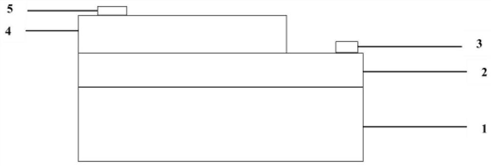
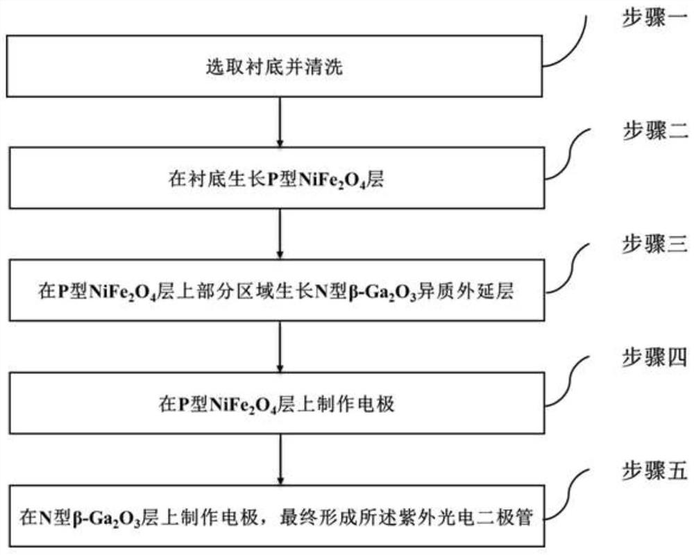
[0054] A NiFe-based 2 o 4 / Ga 2 o 3 The preparation method of the ultraviolet photodiode, flow chart such as figure 2 As shown, the specific steps are as follows:

[0055] Step 1, cleaning the substrate 1, and drying it with nitrogen gas for later use;

[0056] The cleaning process in step 1 is: use cleaning solution-acetone-alcohol-deionized water to clean the sample step by step.

[0057] Step 2, carry out P-type NiFe on the substrate 1 after step 1 cleaning 2 o 4 layer growth;

[0058] P-type NiFe on substrate 1 in step 2 2 o 4 Magnetron sputtering equipment is used for layer growth, with NiFe 2 o 4 The ceramic material is used as the target material, with argon Ar and oxygen O 2 As a sputtering gas, Ar:O during sputtering 2 The ratio is 10:1, the substrate temperature is 500°C, the sputtering pressure is controlled at 0.5Pa, the sputtering power is controlled at 100W, and the sputtering time is controlled at 0.1 hour, and then the sputtered samples are anneal...

Embodiment 2

[0071] A NiFe-based 2 o 4 / Ga 2 o 3 The preparation method of the ultraviolet photodiode, flow chart such as figure 2 As shown, the specific steps are as follows:

[0072] Step 1, cleaning the substrate 1, and drying it with nitrogen gas for later use;

[0073] The cleaning process in step 1 is: use cleaning solution-acetone-alcohol-deionized water to clean the sample step by step.

[0074] Step 2, carry out P-type NiFe on the substrate 1 after step 1 cleaning 2 o 4 layer growth;

[0075] P-type NiFe on substrate 1 in step 2 2 o 4 Magnetron sputtering equipment is used for layer growth, with NiFe 2 o 4 The ceramic material is used as the target material, with argon Ar and oxygen O 2 As a sputtering gas, Ar:O during sputtering 2 The ratio is 5:1, the substrate temperature is 600°C, the sputtering pressure is 5Pa, the sputtering power is 200W, and the sputtering time is 5 hours. After that, the sputtered samples are annealed in the air environment. The temperature...

Embodiment 3

[0088] A NiFe-based 2 o 4 / Ga 2 o 3 The preparation method of the ultraviolet photodiode, flow chart such as figure 2 As shown, the specific steps are as follows:

[0089] Step 1, cleaning the substrate 1, and drying it with nitrogen gas for later use;

[0090] The cleaning process in step 1 is: use cleaning solution-acetone-alcohol-deionized water to clean the sample step by step.

[0091] Step 2, carry out P-type NiFe on the substrate 1 after step 1 cleaning 2 o 4 layer growth;

[0092] P-type NiFe on substrate 1 in step 2 2 o 4 Magnetron sputtering equipment is used for layer growth, with NiFe 2 o 4 The ceramic material is used as the target material, with argon Ar and oxygen O 2 As a sputtering gas, Ar:O during sputtering 2 The ratio is 8:1, the substrate temperature is 550°C, the sputtering pressure is 3Pa, the sputtering power is 150W, and the sputtering time is 3 hours. After that, the sputtered samples are annealed in the air environment. The temperature...


PUM

PropertyMeasurementUnit
thicknessaaaaaaaaaa
thicknessaaaaaaaaaa
thicknessaaaaaaaaaa

Abstract

The invention discloses an ultraviolet photodiode based on NiFe2O4/Ga2O3, and also discloses a preparation method of the ultraviolet photodiode based on NiFe2O4/Ga2O3, which comprises the following steps: cleaning a substrate, and blow-drying the substrate with nitrogen for later use; growing a P-type NiFe2O4 layer on the cleaned substrate; growing an N-type beta Ga2O3 layer in a partial region onthe obtained P-type NiFe2O4 layer; preparing an electrode on the P-type NiFe2O4 layer on the obtained P-type NiFe2O4 layer; and preparing an electrode on the N-type betaGa2O3 layer on the obtained N-type betaGa2O3 layer, and finally forming the ultraviolet photodiode based on NiFe2O4/Ga2O3. According to the invention, the problem that a Ga2O3-based pn junction ultraviolet photodiode cannot be prepared due to the lack of a p-type Ga2O3 material in the prior art is solved.

Description

technical field [0001] The invention belongs to the field of ultraviolet photoelectric detection application technology, in particular to a NiFe-based 2 o 4 / Ga 2 o 3 UV photodiodes, the invention also relates to NiFe-based 2 o 4 / Ga 2 o 3 The fabrication method of the ultraviolet photodiode. Background technique [0002] Gallium oxide (β-Ga 2 o 3 ) as a new type of semiconductor material with direct bandgap and wide bandgap, its bandgap width is 4.9eV, and the corresponding absorption wavelength is 253nm. It has great application potential. At the same time, gallium oxide's high band gap and high breakdown electric field strength (the theoretical value of the critical breakdown electric field strength can reach 8MV / cm), makes gallium oxide deep ultraviolet solar-blind photodetectors more suitable for high-frequency, high-temperature, high-voltage and applications in high radiation environments. [0003] Currently, Ga 2 o 3 UV photodetectors are mainly based on...

Claims


Application Information

Patent Timeline
Patent Type & Authority Applications(China)
IPC IPC(8): H01L31/109H01L31/032H01L31/18
CPCH01L31/109H01L31/032H01L31/18
Inventor 胡继超许蓓贺小敏臧源李连碧
Owner 西安千月电子科技有限公司
Why Eureka
Try Eureka