Unlock instant, AI-driven research and patent intelligence for your innovation.

Reference voltage buffer circuit

A reference voltage buffer, circuit technology, applied in electrical components, physical parameter compensation/prevention, code conversion, etc., can solve problems such as harmonic distortion of output results

Active Publication Date: 2020-12-15
SHENZHEN GOODIX TECH CO LTD
View PDF7 Cites 0 Cited by
  • Summary
  • Abstract
  • Description
  • Claims
  • Application Information

AI Technical Summary

Problems solved by technology

If the reference voltage of the ADC is not fully established, the establishment error will be directly introduced into the ADC output and cause harmonic distortion of the output result

Method used


Image

  • Reference voltage buffer circuit
  • Reference voltage buffer circuit
  • Reference voltage buffer circuit

Examples


Embodiment Construction

[0070] The technical solutions in the embodiments of the present application will be described below with reference to the accompanying drawings.

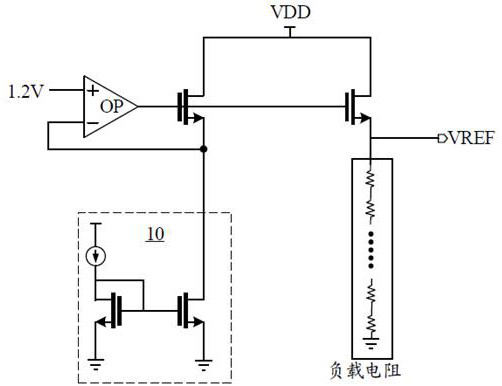
[0071] figure 1 A circuit diagram of a conventional reference voltage buffer (Reference Voltage Buffer, RVB) is shown. Such as figure 1 As shown, the circuit includes an operational amplifier OP on the left, and the output terminal of the operational amplifier is connected to the gates of two MOS transistors, wherein the operational amplifier OP and the left MOS transistor form a feedback branch, which can clamp the right MOS transistor The output voltage of the source VREF , the output voltage can be used as the reference voltage of the ADC; for example, figure 1 The two MOS tubes in are both N-type MOS tubes. Such as figure 1 As shown, the circuit also includes a current source 10 for providing current to the circuit, for example, the current source can be as figure 1 As shown, two metal-oxide-semiconductor (Metal-Oxide-Se...


PUM


Abstract

The embodiment of the invention relates to a reference voltage buffer circuit, and the circuit comprises at least one output branch, wherein each output branch comprises a delay control branch, a first MOS transistor and a second MOS transistor; and a feedback branch. In a first time period, the first end of the feedback branch is used for outputting a first voltage to the delay control branch, and the delay control branch is used for controlling the first MOS transistor and the second MOS transistor to be conducted based on the first voltage, so that the source electrode of the first MOS transistor continuously outputs a reference voltage; in a second time period after the first time period, the voltage output to the delay control branch by the first end of the feedback branch is 0, the delay control branch is used for controlling the first MOS transistor to be switched off and controlling the second MOS transistor to be switched off before the first MOS transistor is switched off, and the voltage output by the source electrode of the first MOS transistor is 0. According to the reference voltage buffer circuit provided by the embodiment of the invention, the reliability of the reference voltage buffer circuit can be improved.

Description

technical field [0001] The embodiments of the present application relate to the field of electronic devices, and more specifically, relate to a reference voltage buffer circuit. Background technique [0002] In order to obtain higher energy efficiency, the capacitive successive approximation register (Successive Approximation Register, SAR) architecture is often used in the design of a medium-to-high-speed, medium-to-high-precision analog-to-digital converter (Analog to Digital Converter, ADC). However, when each bit in the SAR algorithm is generated, a capacitive digital-to-analog converter (CapacitorDigital to Analog Converter, CDAC) needs to extract some signal-related charge from the reference voltage. If the reference voltage of the ADC is not fully established, the establishment error will be directly introduced into the ADC output and cause harmonic distortion of the output result. Therefore, in order to reduce the harmonic distortion caused by the establishment erro...

Claims


Application Information

Patent Timeline
IPC IPC(8): H03M1/06
CPCH03M1/0614
Inventor 陈俊熹汪正锋
Owner SHENZHEN GOODIX TECH CO LTD
Features
  • R&D
  • Intellectual Property
  • Life Sciences
  • Materials
  • Tech Scout
  • Unparalleled Data Quality
  • Higher Quality Content
  • 60% Fewer Hallucinations
Learn More