
A full-color active addressable micro-led chip structure and manufacturing method thereof

A chip structure and addressing technology, applied to semiconductor devices, electrical components, circuits, etc., can solve the problems of large number of electrode leads and poor chip efficiency, and achieve the goal of reducing the difficulty of chip manufacturing, enhancing the uniformity of current distribution, and improving efficiency Effect

Active Publication Date: 2021-09-17
XIAMEN UNIV
View PDF7 Cites 0 Cited by
  • Summary
  • Abstract
  • Description
  • Claims
  • Application Information

AI Technical Summary

Problems solved by technology

[0006] The main purpose of the present invention is to overcome the defect that the vertically stacked full-color Micro-LED chip has a large number of electrode leads in the prior art, which leads to poor chip efficiency, and proposes a full-color active addressable Micro-LED chip structure and its Production Method

Method used


Image

  • A full-color active addressable micro-led chip structure and manufacturing method thereof
  • A full-color active addressable micro-led chip structure and manufacturing method thereof
  • A full-color active addressable micro-led chip structure and manufacturing method thereof

Examples


Embodiment Construction

[0046] The present invention will be further described below through specific embodiments.

[0047] Terms such as "first" and "second" appearing in the present invention are only for convenience of description, to distinguish different components with the same name, and do not indicate a sequence or a primary and secondary relationship. In the description, the orientation or positional relationship indicated by "upper", "lower", "left", "right", "front" and "rear" is based on the orientation or positional relationship shown in the drawings, and is only for the purpose of It is convenient to describe the present invention, but does not indicate or imply that the referred device must have a specific orientation, be constructed and operate in a specific orientation, and thus should not be construed as limiting the protection scope of the present invention.

[0048] In the present invention, the terms "first", "second", "third" and so on are only used to distinguish similar object...


PUM


Abstract

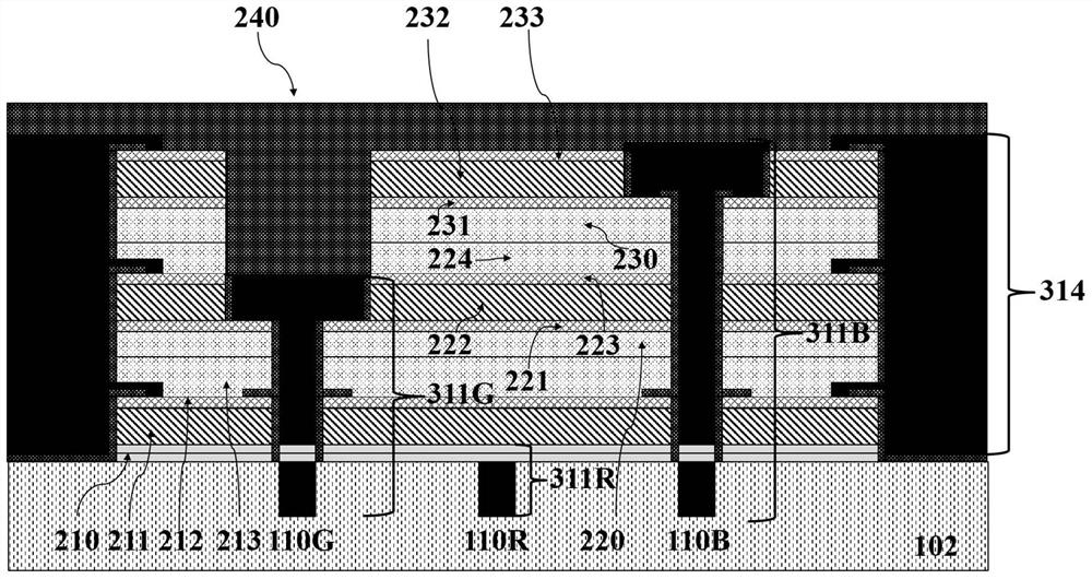
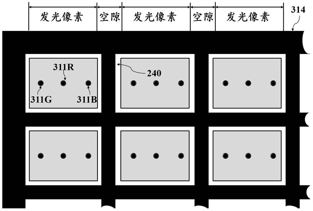
The present invention relates to a full-color active addressable Micro-LED chip structure and a manufacturing method thereof, comprising a supporting substrate with a driving circuit array, a stacked layer on the supporting substrate, and a through-stacked layer connected to the driving circuit array Interconnected electrodes, wherein the stacked layers include a substrate metal bonding layer, a multi-layer sandwich structure covered with a transparent conductive layer on the upper and lower surfaces of the multicolor light-emitting epitaxial layer, a dielectric filling layer, a filter layer, a passivation layer, and interconnected electrodes from bottom to top. It includes an array electrode connecting the p-type surface of the first epitaxial layer and the driving pixel, a penetrating array electrode connecting the p-type surface of the second epitaxial layer and the driving pixel, a penetrating array electrode connecting the p-type surface of the third epitaxial layer and the driving pixel, and a penetrating array electrode connecting the p-type surface of the third epitaxial layer and the driving pixel. The stacked layers are respectively connected to the common electrode of the n-type surface of the multi-color light-emitting epitaxial layer. The technical solution of the present invention can manufacture high-resolution and high-efficiency full-color drive fusion Micro-LED chips.

Description

technical field [0001] The invention relates to the technical field of semiconductor optoelectronic devices, in particular to a full-color active addressable Micro-LED chip structure and a manufacturing method thereof. Background technique [0002] As an active light-emitting display technology, each red, green and blue sub-pixel of Micro-LED is an independently adjustable light source. Micro-LED not only has high contrast ratio, high speed and wide viewing angle similar to organic light emitting diode (OLED), but also can provide wider color gamut, higher brightness, lower power consumption, longer service life, stronger durability and environmental stability. In addition, Micro-LEDs can integrate sensors and electronic circuits to form thin-film displays, embedded in sensing systems such as fingerprint recognition and gesture control. Therefore, Micro-LED display technology has broad application prospects in various consumer applications such as wearable devices, augment...

Claims


Application Information

Patent Timeline
Patent Type & Authority Patents(China)
IPC IPC(8): H01L33/38H01L27/15H01L33/00
CPCH01L27/156H01L33/005H01L33/387H01L2933/0016
Inventor 杨旭李金钗李书平康俊勇
Owner XIAMEN UNIV
Learn More