Micro-nano structure processing method and system with array anti-reflection and anti-reflection functions
A technology of micro-nano structure and processing method, which is applied in the direction of metal processing equipment, manufacturing tools, welding equipment, etc., can solve the problems of poor precision, consistency, and low efficiency, and achieve the goal of improving manufacturing efficiency, improving manufacturing efficiency, and ensuring manufacturing accuracy Effect
- Summary
- Abstract
- Description
- Claims
- Application Information
AI Technical Summary
Problems solved by technology
Method used
Image
Examples
Embodiment 1
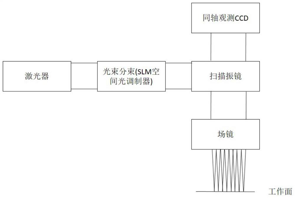
[0081] The system composition used in this embodiment is as follows: figure 1 As shown, it is composed of laser, SLM spatial light modulator, scanning galvanometer, field mirror and coaxial observation CCD and other components. In other embodiments, the field lens can also be replaced by a microscope objective lens.
[0082] The output laser light of the laser enters the SLM spatial light modulator, and the SLM spatial light modulator divides the laser beam into array processing beams, which are reflected to the field mirror by the scanning galvanometer, and the array processing beams are focused to the working surface by the field mirror, realizing the array micro nanostructure processing.
[0083] The specific method is realized through the following steps:
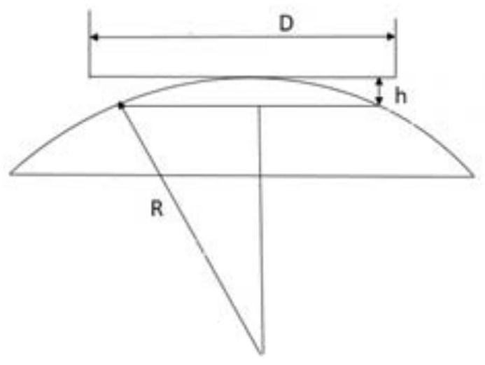
[0084] (1) Carry out process tests to determine the adjustable range h of each micro-nano structure. The micro-nano structure can be a blind hole on the surface of the workpiece, and the radial section of the hole ca...
Embodiment 2
[0112] The system adopted in this embodiment adds a Fesnel lens on the basis of the embodiment, and the laser is shaped into an array Bessel processing beam through the SLM spatial light modulator, and the array Bessel processing beam is realized by superimposing the Fesnel lens. Not at the same position (realize three-dimensional shaping of laser space), the working surface of the beam is directly shaped into a shape distributed along the surface shape of the component. Compared with the first embodiment, the processing process does not need to consider the manufacturing adjustable range h. Such as Figure 8 shown.
[0113] The specific method is realized through the following steps:
[0114] (1) Divide the surface part to be processed into several sub-regions:
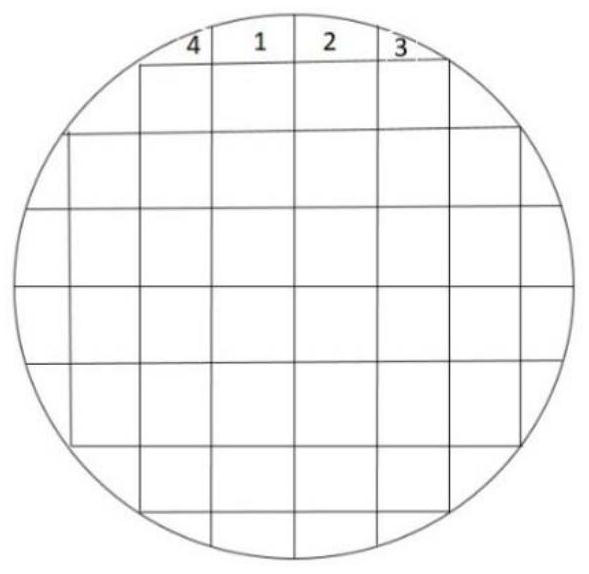
[0115] Such as Figure 8 In b, based on the requirement that the scanning galvanometer can scan the maximum range D at one time, the curved surface part is divided into several sub-areas, and the maximum side leng...
PUM
 Abstract
Description
Claims
Application Information


