Method for improving bursting of film layer, and film material

A thin-film material and thin-film layer technology, applied in piezoelectric/electrostrictive/magnetostrictive devices, electrical components, circuits, etc., can solve the problem of easy cracking of the thin-film layer, improve the cracking of the thin-film layer, and solve the cracking of the thin-film layer. Effect

Active Publication Date: 2021-01-22
JINAN JINGZHENG ELECTRONICS
View PDF10 Cites 1 Cited by
  • Summary
  • Abstract
  • Description
  • Claims
  • Application Information

AI Technical Summary

Problems solved by technology

[0005] In order to solve the problem that in the prior art, when heat-treating the bonding body between the non-homogeneous thin-film wafer and the substrate layer, the thin-film wafer and the substrate layer have different thermal expansion coefficients during annealing and separation, and the thin-film layer is easy to burst after bonding and separation. , the application provides a method for improving the cracking of the film layer

Method used


Image

  • Method for improving bursting of film layer, and film material
  • Method for improving bursting of film layer, and film material
  • Method for improving bursting of film layer, and film material

Examples


Embodiment Construction

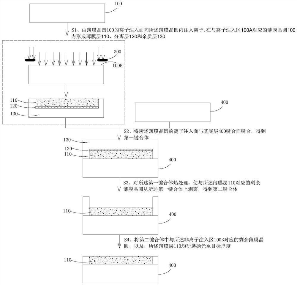
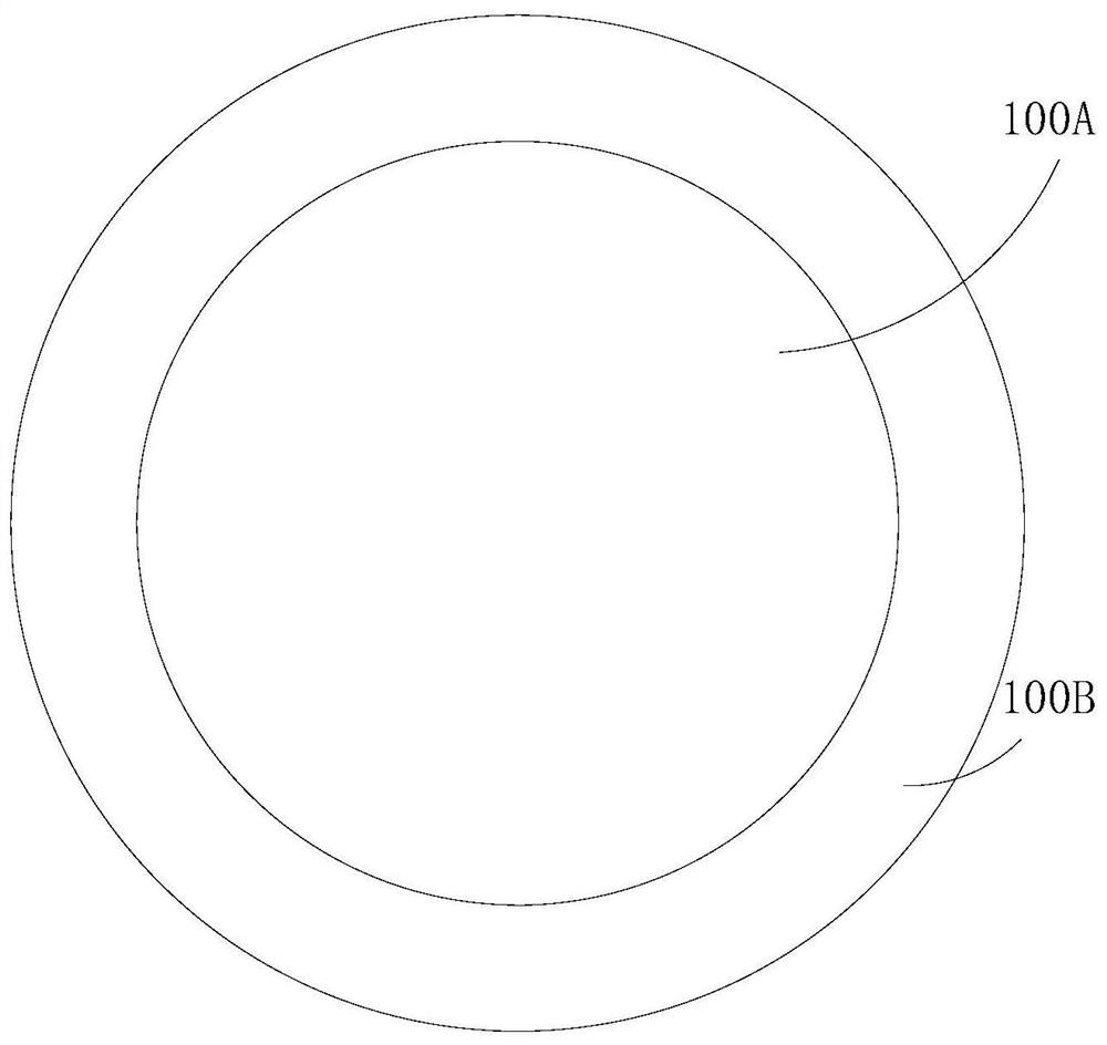
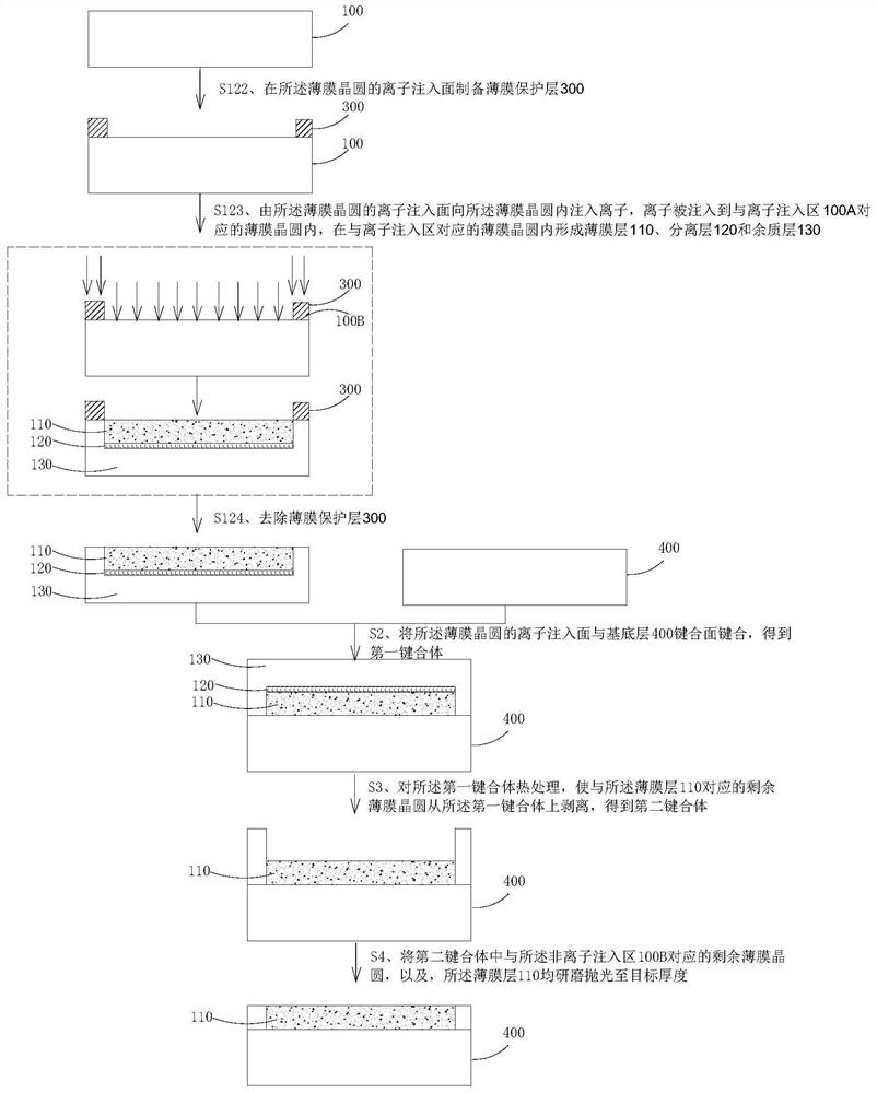
[0041] In order to make those skilled in the art better understand the solutions of the present invention, the technical solutions in the embodiments of the present invention will be clearly and completely described below with reference to the accompanying drawings in the embodiments of the present invention. Obviously, the described embodiments are only These are some embodiments of the present invention, but not all embodiments. Based on the embodiments of the present invention, all other embodiments obtained by those skilled in the art without creative efforts shall fall within the protection scope of the present invention.

[0042] The word "exemplary" is used exclusively herein to mean "serving as an example, embodiment, or illustration." Any embodiment described herein as "exemplary" is not necessarily to be construed as preferred or advantageous over other embodiments. While various aspects of the embodiments are shown in the drawings, the drawings are not necessarily ...


PUM


Abstract

The invention discloses a method for improving bursting of a film layer, and a film material. The method comprises the following steps: injecting ions into a film wafer from an ion implantation surface of the film wafer, and forming the film layer, a separation layer and a remainder layer in the part, corresponding to an ion injection region, of the film wafer; bonding an ion implantation surfaceof the film wafer with a bonding surface of a substrate layer to obtain a first bonding body; performing heat treatment on the first bonding body to obtain a second bonding body; and grinding and polishing a remaining film wafer part corresponding to a non-ion implantation region in the second bonding body and the film layer to a target thickness. According to the invention, a circle of non-ion implantation region is reserved at the periphery of the ion implantation region, so after ion implantation, the film layer and the separation layer are only formed in the part, corresponding to the ionimplantation region, of the film wafer; and therefore, during bonding separation, due to the existence of the remaining thin film wafer part corresponding to the non-ion implantation region, the filmlayer is prevented from instantaneously recovering to a flat state from a warping state, and the problem of bursting of the film layer is solved.

Description

technical field [0001] The present application belongs to the field of semiconductor element preparation, and in particular relates to a method and a thin film material for improving the bursting of a thin film layer. Background technique [0002] Thin film wafers such as lithium niobate or lithium tantalate are widely used in nonlinear optics, ferroelectric, piezoelectric, etc. due to their high Curie temperature, strong spontaneous polarization, high electromechanical coupling coefficient, and excellent electro-optic effect , electro-optic and other fields. At present, the methods for preparing lithium niobate or lithium tantalate films mainly include epitaxial growth method, ion implantation and bonding separation method, ion implantation and grinding and polishing method. [0003] Among them, the method for preparing the thin film by ion implantation and bonding separation method mainly includes the following steps: firstly, implanting ions into a thin film wafer such a...

Claims


Application Information

Patent Timeline
IPC IPC(8): H01L41/312H01L41/331H01L21/265
CPCH01L21/265H10N30/072H10N30/081
Inventor 张涛朱厚彬张秀全
Owner JINAN JINGZHENG ELECTRONICS
Why Eureka
Try Eureka