GaSe nano-material, liquid phase stripping method and application of method
A technology of nanomaterials and liquid phase exfoliation, applied in the field of two-dimensional materials, can solve the problems of high time and equipment requirements, and achieve the effect of low cost, uniform dispersion and clear shape
- Summary
- Abstract
- Description
- Claims
- Application Information
AI Technical Summary
Problems solved by technology
Method used
Image
Examples
Embodiment 1
[0049] Step 1: Prepare 50 mg of GaSe with a purity of 99.995%.
[0050] Step 2: Weigh 2ml of IPA with a purity of 99.7% and put it into a transparent glass dispensing bottle, add the GaSe weighed in Step 1 into the IPA solution, and seal the glass bottle.
[0051] Step 3: Place the sealed glass bottle in an ultrasonic equipment with a power of 300W and a frequency of 40kHz in a water bath for 3-4 hours, keep the bath temperature at 25°C, and carry out ultrasonic dispersion. The speed of ultrasonic dispersion is 8000-10000rpm, and finally the initial dispersion is obtained liquid.
[0052] Step 4: Add 2 ml of IPA isopropanone to the initial dispersion liquid, place it in a water bath, centrifuge at a speed of 10,000 rpm for 3 min, and separate the supernatant for use.
[0053] Step 5: Put the supernatant separated in step 4 into an ultrasonic equipment with a power of 300W and a frequency of 40kHz in a water bath for 2 hours, keep the bath temperature at 25°C, and then centrif...
example 1
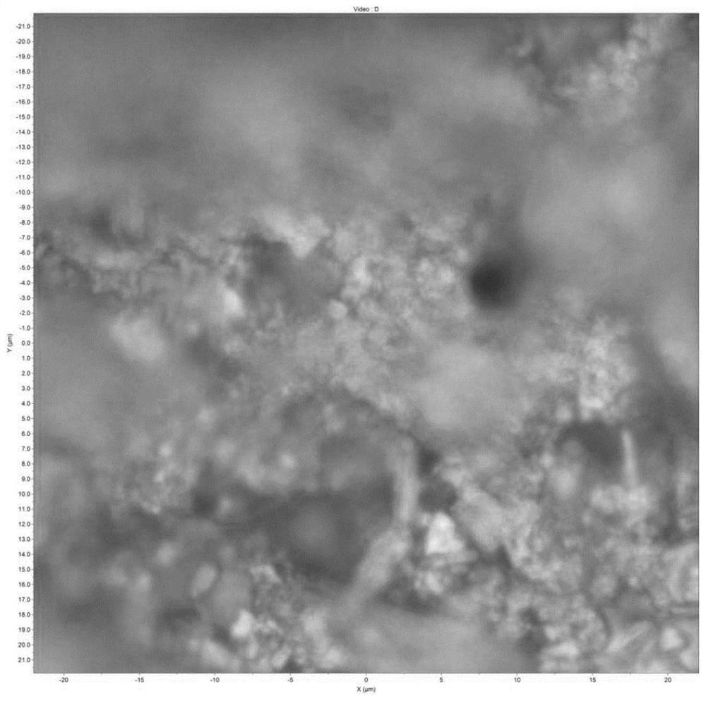
[0054] The optical spectrum of the used GaSe granular material of example one is as figure 1 As shown, the obtained Raman spectrum is shown as Figure 9 shown;
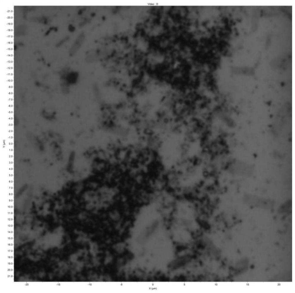
[0055]Optical photographs of the resulting GaSe nanomaterials as figure 2 As shown, the Raman spectrum is as Figure 10 As shown, the AFM spectrum is as Figure 18 shown;
[0056] figure 1 and figure 2 It shows that the thickness of the obtained product is thicker, the shape is irregular sheet, and the yield is more.
[0057] Figure 9 , Figure 10 and Figure 18 It shows that the obtained product is a GaSe nanomaterial and the thickness of its single layer is thinned to 8.727nm. According to the literature (Tang Luping. CVD preparation of gallium selenide nanostructure and research on its photoelectric properties [D].), it can be judged that the number of layers is 8-9 layer, the resulting flakes piled up severely.
Embodiment 2
[0059] Step 1: Same as Embodiment 1.
[0060] Step 2: Same as Embodiment 1.
[0061] Step 3: Place the sealed glass bottle in a water bath for 3-4 hours in an ultrasonic device with a power of 300W and a frequency of 40kHz, and keep the bath temperature at 35°C.
[0062] Step 4: Same as Embodiment 1.
[0063] Step 5: Put the supernatant separated in step 4 into an ultrasonic equipment with a power of 300W and a frequency of 40kHz in a water bath for 2 hours, keep the bath temperature at 35°C, and then centrifuge the dispersion at 10,000 rpm for 3 minutes to separate the supernatant liquid.
[0064] The color of the supernatant obtained from the reaction is lighter than that in Example 1.
PUM
| Property | Measurement | Unit |
|---|---|---|
| thickness | aaaaa | aaaaa |
| thickness | aaaaa | aaaaa |
| thickness | aaaaa | aaaaa |
Abstract
Description
Claims
Application Information


