Bias frequency mixing Schottky diode structure and semiconductor device

A technology of Schottky diode and Schottky junction, which is applied in the direction of semiconductor devices, electrical components, circuits, etc., can solve the problem of difficulty in realizing the vibration source, and achieve the effect of reducing difficulty and reducing the demand for local oscillator power

Active Publication Date: 2021-01-29
THE 13TH RES INST OF CHINA ELECTRONICS TECH GRP CORP
View PDF6 Cites 3 Cited by
  • Summary
  • Abstract
  • Description
  • Claims
  • Application Information

AI Technical Summary

Problems solved by technology

[0004]The purpose of the present invention is to provide a biasable frequency mixing Schottky diode st

Method used


Image

  • Bias frequency mixing Schottky diode structure and semiconductor device
  • Bias frequency mixing Schottky diode structure and semiconductor device

Examples


Embodiment Construction

[0020] In order to make the technical problems, technical solutions and beneficial effects to be solved by the present invention clearer, the present invention will be further described in detail below in conjunction with the accompanying drawings and embodiments. It should be understood that the specific embodiments described here are only used to explain the present invention, not to limit the present invention.

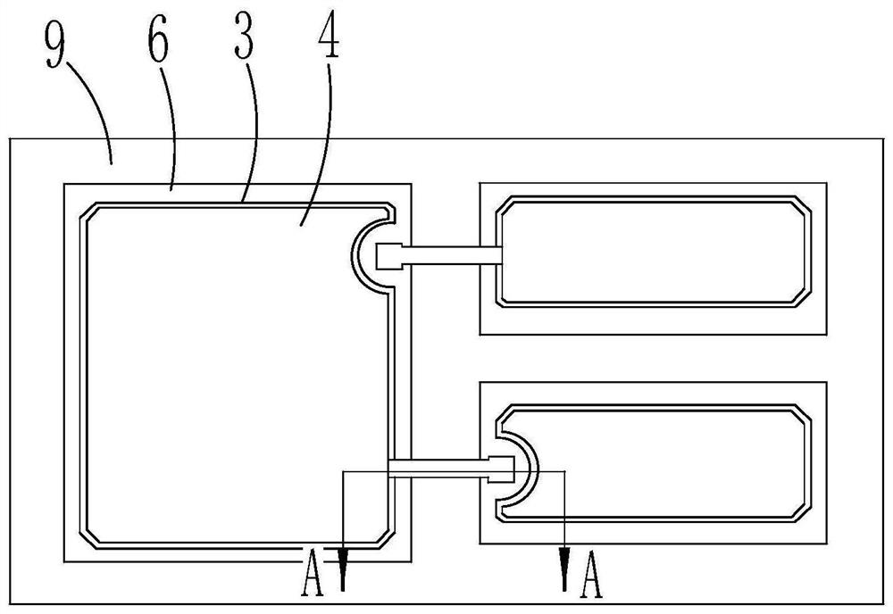
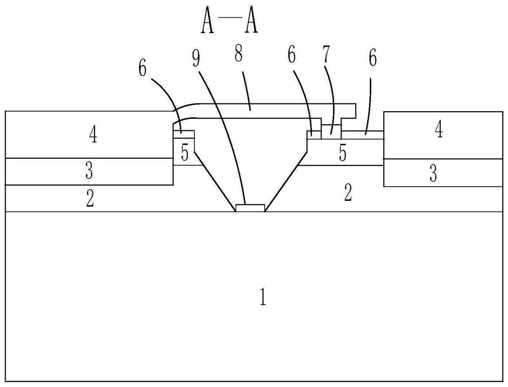
[0021] see figure 1 , the biasable frequency mixing Schottky diode structure provided by the present invention will now be described. The biasable frequency mixing Schottky diode structure includes a first metal electrode and a second metal electrode, the second metal electrode is divided into an upper sub-electrode and a lower sub-electrode, and the first Schottky junction is connected to the Between the first metal electrode and the upper sub-electrode, the second Schottky junction is connected in antiparallel between the first metal electrode and the lower sub-...


PUM

PropertyMeasurementUnit
Doping concentrationaaaaaaaaaa

Abstract

The invention provides a bias frequency mixing Schottky diode structure and a semiconductor device, and belongs to the technical field of semiconductor devices. The bias frequency mixing Schottky diode structure comprises a first metal electrode and a second metal electrode, the second metal electrode is divided into an upper sub-electrode and a lower sub-electrode, a first Schottky junction is connected between the first metal electrode and the upper sub-electrode, and the second Schottky junction is reversely connected in parallel between the first metal electrode and the lower sub-electrode. According to the bias frequency mixing Schottky diode structure provided by the invention, the two Schottky junctions are connected in parallel reversely, one ends of the Schottky junctions are connected with the same metal electrode, and the other ends of the Schottky junctions are connected with the two disconnected metal electrodes so that the diode can be biased, and the requirement of a frequency mixer on local oscillation power is reduced; and the difficulty of a local oscillation source is decreased.

Description

technical field [0001] The invention belongs to the technical field of semiconductor devices, and more specifically relates to a biasable frequency mixing Schottky diode structure and a semiconductor device. Background technique [0002] Terahertz (THz) waves refer to electromagnetic waves with a frequency in the range of 0.3-3THz, between millimeter waves and infrared light. THz waves occupy a very special position in the electromagnetic wave spectrum. They have the characteristics of high frequency, wide bandwidth, and good safety. They are widely used in security inspection, communication, radar, and radio astronomy. [0003] The key to researching terahertz electronic systems is terahertz transmitting and receiving technology. In the terahertz frequency band, due to the lack of corresponding low-noise amplifiers, the terahertz mixer has become the first stage of the receiving end of the electronic system, and its indicators directly affect the performance of the entire ...

Claims


Application Information

Patent Timeline
IPC IPC(8): H01L29/872H01L29/06H01L29/47
CPCH01L29/872H01L29/0688H01L29/475
Inventor 张立森梁士雄杨大宝宋旭波徐鹏吕元杰顾国栋冯志红
Owner THE 13TH RES INST OF CHINA ELECTRONICS TECH GRP CORP
Why Eureka
Try Eureka