A kind of packing method of LED core particle and LED core particle packing structure

A packaging method and packaging structure technology, applied in the manufacturing of semiconductor devices, electrical components, semiconductor/solid-state devices, etc., can solve the problems of uneven brightness and darkness of the outer ring core particles, identification and other problems, and achieve high efficiency, low cost, and reduced The effect of the alarm

Active Publication Date: 2022-02-22
XIAMEN SANAN OPTOELECTRONICS CO LTD
View PDF3 Cites 0 Cited by
  • Summary
  • Abstract
  • Description
  • Claims
  • Application Information

AI Technical Summary

Problems solved by technology

[0004] The present invention aims to provide a packaging method for LED core particles to solve the problem that the existing outer ring core particles cannot be recognized by the automatic image recognition visual system of the die-bonding machine due to uneven brightness and darkness

Method used


Image

  • A kind of packing method of LED core particle and LED core particle packing structure
  • A kind of packing method of LED core particle and LED core particle packing structure
  • A kind of packing method of LED core particle and LED core particle packing structure

Examples


Embodiment 1

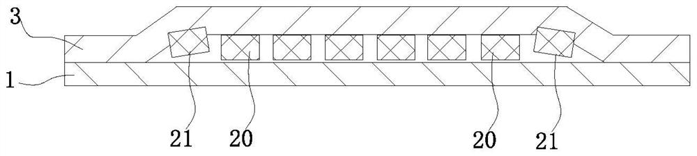
[0029] Such as figure 1 and figure 2 shown. in figure 1 It is a schematic diagram of sticking release paper after the core particles are fixed on the film. exist figure 1 Among them, the number 1 represents the adhesive film, 20 represents the non-outermost non-outer ring core particle, 21 represents the outermost outer ring core particle among all the core particles, and 3 represents the release paper.

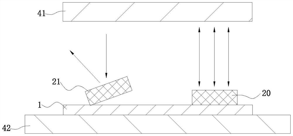
[0030] figure 2 It is a schematic diagram of non-outer ring core particles 20 and outer ring core particles 21 under the CCD lens of the die bonder. exist figure 2 Among them, the reference number 41 represents the CCD lens of the die bonder, and 42 represents the plate of the die bonder, and the arrow in the figure represents the light path.

[0031] The applicant found in the research that the main reason for the uneven brightness and darkness of the outer ring core particles 21 is that the outer ring core particles 21 are affected by the bonding force of the adh...

Embodiment 2

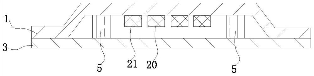
[0043] refer to Figure 3-Figure 5, this embodiment provides an LED chip packaging structure produced by the LED chip packaging method proposed in Example 1, including an adhesive film, a plurality of LED chips, a cover and a support, wherein a plurality of LED The core particles are fixed on the adhesive film 1, and are divided into outer ring core particles 21 located at the edge and non-outer ring core particles 20 located in the outer ring core particles 21 according to their positional relationship; the support is placed on the adhesive film There is fixed on one side of the core particle, the support 5 ring is arranged on the edge of the outermost core particle, and the maximum thickness of the support 5 is greater than the maximum thickness of the core particle;

[0044] The cover covers the support 5 and all the core particles, and is fixed on the adhesive film 1 and / or the support 5, and the support 5 prevents the cover from directly contacting the position of the cor...


PUM


Abstract

The invention relates to a packaging method of LED core particles and a packaging structure of LED core particles. The packaging structure of the method includes adding a support between the adhesive film and the release paper, so that the release paper does not directly contact the position of the core particles. The adhesive film does not generate pressure to cause the outer ring core particles to tilt, so as to solve the problem that the existing outer ring core particles cannot be recognized by the automatic image recognition vision system of the die bonder due to uneven brightness and darkness.

Description

technical field [0001] The invention relates to the field of semiconductor chips, in particular to a packaging method for LED core particles and a packaging structure for LED core particles. Background technique [0002] After the current LED wafer is cut and tested, it will be classified according to the photoelectric parameters such as voltage (VF), wavelength (WLD), optical power (LOP), etc., and the chips with different parameters will be captured by the sorting machine to different film ( In terms of tape), blue film, white film and UV film are mainly used to fix the chip. After sorting, the chip factory pastes release paper on the film and ships it to the packaging factory for chip fixing and wire bonding. [0003] As the size of LED chips becomes smaller and smaller, the size of some chips used in mini LED displays is often less than 100um. When the die-bonding machine in the packaging factory picks up the chips, there will be a circle at the edge (the smaller the chi...

Claims


Application Information

Patent Timeline
Patent Type & Authority Patents(China)
IPC IPC(8): H01L33/48H01L21/683H01L21/67
CPCH01L33/483H01L21/67132H01L21/6836H01L2221/68313H01L2933/0033
Inventor 卢栋梁林宗民陈明湖林维扬林桂绮曾合加蔡吉明
Owner XIAMEN SANAN OPTOELECTRONICS CO LTD
Why Eureka
Try Eureka