Light-emitting diode epitaxial wafer and preparation method thereof

A technology of light-emitting diodes and epitaxial wafers, which is applied in semiconductor devices, electrical components, circuits, etc., can solve the problems of improving the crystal quality of the n-type GaN layer and the p-type GaN layer, so as to improve the luminous efficiency and reduce the formation of dislocations and defects. , the effect of reducing the dislocation density

Active Publication Date: 2022-03-15
HC SEMITEK ZHEJIANG CO LTD
View PDF5 Cites 0 Cited by
  • Summary
  • Abstract
  • Description
  • Claims
  • Application Information

AI Technical Summary

Problems solved by technology

[0004] However, when the GaN buffer layer itself grows on the AlN layer, it will also accumulate some dislocation defects, and these dislocation defects will extend to structures such as the n-type GaN layer, resulting in the final n-type GaN layer, multiple quantum well layer and p The crystal quality of the GaN layer has limited improvement

Method used


Image

  • Light-emitting diode epitaxial wafer and preparation method thereof
  • Light-emitting diode epitaxial wafer and preparation method thereof
  • Light-emitting diode epitaxial wafer and preparation method thereof

Examples


Embodiment Construction

[0034] In order to make the object, technical solution and advantages of the present invention clearer, the implementation manner of the present invention will be further described in detail below in conjunction with the accompanying drawings.

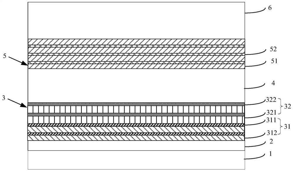
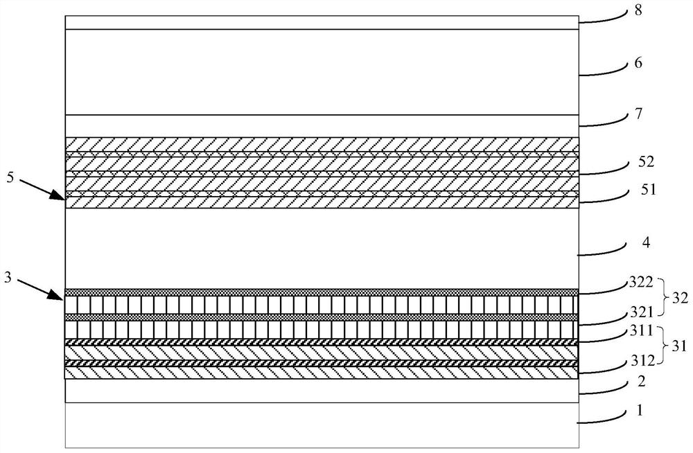
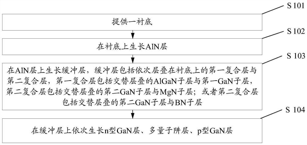
[0035] figure 1 It is a schematic structural diagram of a light-emitting diode epitaxial wafer provided by an embodiment of the present disclosure. Refer to figure 1 It can be seen that the embodiment of the present disclosure provides a light-emitting diode epitaxial wafer, which includes a substrate 1 and an AlN layer 2, a buffer layer 3, an n-type GaN layer 4, and a multi-quantum well layer stacked on the substrate 1 in sequence. 5 and p-type GaN layer 6.

[0036] The buffer layer 3 includes a first composite layer 31 and a second composite layer 32 sequentially stacked on the substrate 1, the first composite layer 31 includes alternately stacked AlGaN sublayers 311 and first GaN sublayers 312, and the second composite layer 32 It...


PUM

PropertyMeasurementUnit
pressureaaaaaaaaaa
thicknessaaaaaaaaaa
thicknessaaaaaaaaaa

Abstract

The invention discloses a light-emitting diode epitaxial wafer and a preparation method thereof, belonging to the field of light-emitting diode production. The alternately stacked AlGaN sub-layers and the first GaN sub-layer can release certain stress during the growth process, and less dislocation defects will be accumulated in the first composite layer. The buffer layer also includes a second composite layer stacked on the first composite layer, and the structure of the second composite layer can be alternately stacked second GaN sublayers and MgN sublayers, alternately stacked second GaN sublayers and BN sublayers . Mg atoms and B atoms in the BN sublayer have small particle sizes, which can fill the vacancies generated by defects and dislocations in the crystal during growth, thereby reducing the formation of dislocations and defects, improving the crystal quality of the buffer layer, and finally obtaining The luminous efficiency of the light-emitting diode epitaxial wafer is also improved.

Description

technical field [0001] The invention relates to the field of light-emitting diode production, in particular to a light-emitting diode epitaxial wafer and a preparation method thereof. Background technique [0002] LED (English: Light Emitting Diode, Chinese: Light Emitting Diode), a light emitting diode is a semiconductor electronic component that can emit light. As an efficient, environmentally friendly and green new solid-state lighting source, it is being rapidly and widely used, such as traffic lights, car interior and exterior lights, urban landscape lighting, mobile phone backlight, etc. Improving the luminous efficiency of chips is the goal that LEDs are constantly pursuing. [0003] The epitaxial wafer of a light emitting diode usually includes a substrate and an AlN layer, a GaN buffer layer, an n-type GaN layer, a multi-quantum well layer and a p-type GaN layer grown sequentially on the substrate. The GaN buffer layer can alleviate the lattice mismatch between the...

Claims


Application Information

Patent Timeline
Patent Type & Authority Patents(China)
IPC IPC(8): H01L33/12H01L33/06H01L33/00
CPCH01L33/12H01L33/06H01L33/007
Inventor 洪威威王倩梅劲董彬忠吕蒙普
Owner HC SEMITEK ZHEJIANG CO LTD
Why Eureka
Try Eureka