

A gan HEMT device with high breakdown voltage
A technology with high breakdown voltage and high resistance, applied in electrical components, semiconductor devices, circuits, etc., can solve the problem of low breakdown voltage, achieve high breakdown voltage, increase threshold voltage, and improve breakdown voltage Effect
- Summary
- Abstract
- Description
- Claims
- Application Information
AI Technical Summary
Problems solved by technology
Method used
Image

Examples
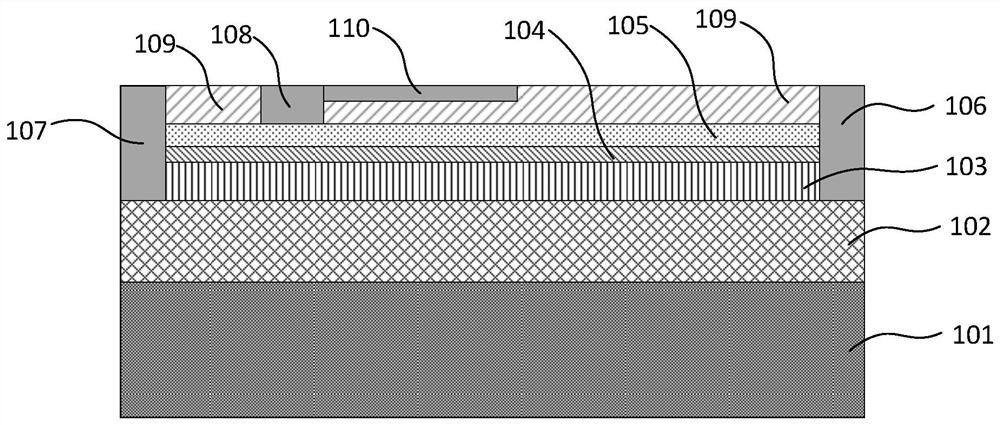
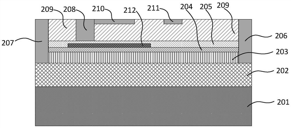
Embodiment 1
[0034] This embodiment 1 provides a GaN HEMT device with a gate segmented field plate and a polarization layer under the gate, and its structural diagram is as follows image 3 As shown, including a second substrate 201, a second GaN buffer layer 202, a second GaN channel layer 203, a second AlGaN barrier layer 204, a second gate dielectric layer 205 and SiO 2 The second passivation layer 209 is provided with a source electrode 207 and a drain electrode 206 at both ends above the GaN buffer layer 202, and a gate electrode 208 is arranged on the gate dielectric layer 205 close to the source electrode 207. The dielectric layer 205 is provided with a lower gate polarization layer 212, which is directly in contact with the lower AlGaN barrier layer 204. The starting point of one side of the gate lower polarization layer 212 is located at the side of the gate electrode 208, and the other side is terminated. The end point is located on the other side of the gate electrode 208; the s...
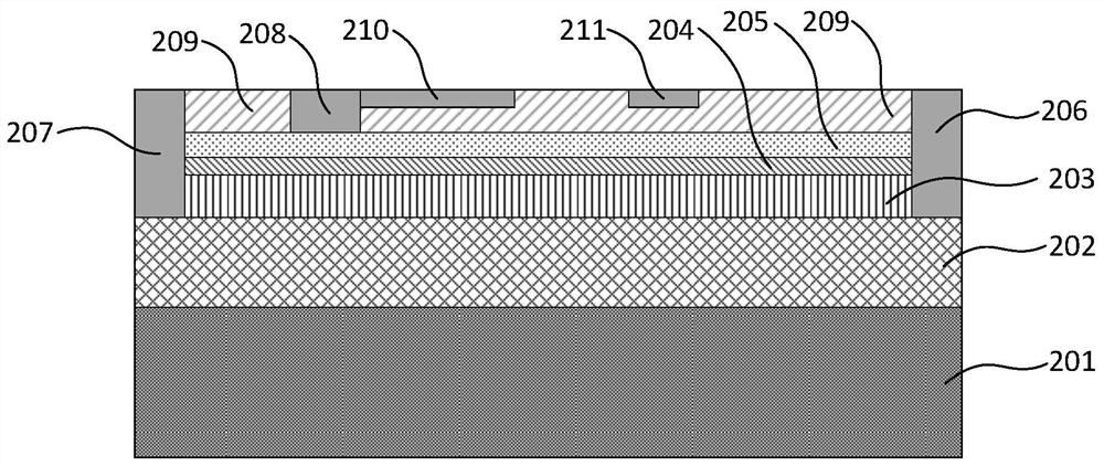
Embodiment 2
[0039] Embodiment 2 provides a GaN HEMT device with a gate segmented field plate and a polarized layer under the gate. The difference between Embodiment 2 and Embodiment 1 is that the left end of the polarized layer 212 under the gate starts At 0 μm on the right side of the electrode 208, other parameters are the same as those in Embodiment 1.
experiment example 1
[0053] Through simulation, the distribution comparison diagram of the channel electric field along the horizontal direction when the GaN HEMT device breaks down in Example 1 and Comparative Example 1, Comparative Examples 1 and 2, and the channel electric field along the horizontal direction when the GaN HEMT device breaks down in Comparative Example 1 The distribution diagram, the experimental results are as follows Figure 7 , Figure 6 as well as Figure 5 shown.
[0054] Depend on Figure 5 The distribution diagram of the channel electric field along the horizontal direction when the traditional device using gate field plate technology breaks down shows that after using the gate field plate, the peak value of the channel electric field is 2.1MV / cm at the right edge of the gate electrode with X=5μm , lower than the critical breakdown electric field of GaN material, the electric field distribution of the channel is relatively uniform, and the withstand voltage value of th...
PUM
| Property | Measurement | Unit |
|---|---|---|
| thickness | aaaaa | aaaaa |
| length | aaaaa | aaaaa |
| length | aaaaa | aaaaa |
Abstract
Description
Claims
Application Information