Novel SPI-NAND Flash memory chip with DDR high transmission interface and operation method
A memory chip and high-transmission technology, applied in the field of new SPI-NAND Flash memory chips, can solve the problems of not being able to support DDR2, MLCNANDFlashDieSize cannot be packaged, etc.
- Summary
- Abstract
- Description
- Claims
- Application Information
AI Technical Summary
Problems solved by technology
Method used
Image
Examples
Embodiment Construction
[0031] In order to make the object, technical solution and advantages of the present invention clearer, the present invention will be described in detail below with reference to the accompanying drawings and specific embodiments.
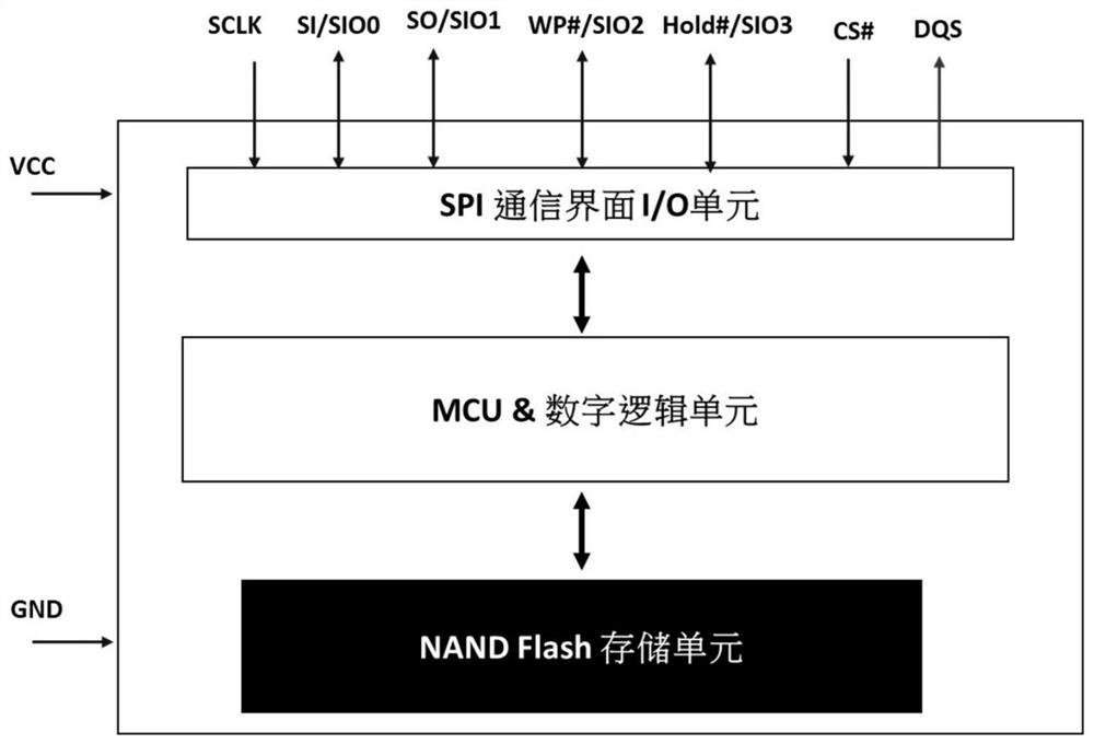
[0032] Since SPI-NAND Flash is a passive memory chip, in the current operation mode, there are strict operation commands to read and write data. In order to meet the needs of increasing transmission speed, NV-DDR2 technology is used in the existing SPI-NADN On the basis of the Flash memory chip, the DDR mode is added to increase the reading speed by 2 times. It is used to speed up the reading of data, and one Clock clock is used as the transmission unit, which is reduced to half a Clock clock as the transmission unit. The description of the SPI-NAND Flash memory chip is as follows:
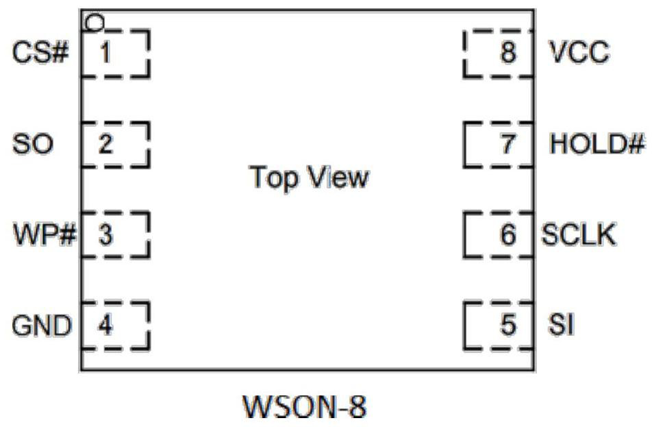
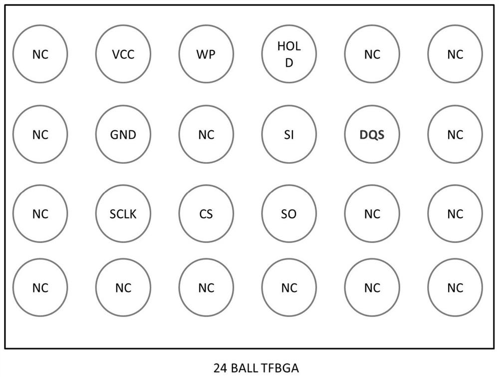
[0033] like figure 1 and Figure 10 As shown, a new type of SPI-NAND Flash memory chip with a high transmission interface, including: SPI command logic control unit, ...
PUM
 Abstract
Description
Claims
Application Information


