Surface plasmon induced electron emission source

A surface plasmon, electron emission source technology, applied in the field of electronics, can solve the problems of low brightness and low imaging resolution

Active Publication Date: 2021-02-26
TSINGHUA UNIV
View PDF8 Cites 0 Cited by
  • Summary
  • Abstract
  • Description
  • Claims
  • Application Information

AI Technical Summary

Problems solved by technology

[0005] An embodiment of the present invention provides a surface plasmon-induced electron emission source, which is used to solve the defect of low imaging resolution in the prior art, realize the emission of electron beams with high energy dispersion and low brightness, and improve the performance of LV-SEM. Imaging resolution

Method used


Image

  • Surface plasmon induced electron emission source
  • Surface plasmon induced electron emission source
  • Surface plasmon induced electron emission source

Examples


Embodiment Construction

[0025] In order to make the purpose, technical solutions and advantages of the embodiments of the present invention clearer, the technical solutions in the embodiments of the present invention will be clearly and completely described below in conjunction with the drawings in the embodiments of the present invention. Obviously, the described embodiments It is a part of embodiments of the present invention, but not all embodiments. Based on the embodiments of the present invention, all other embodiments obtained by persons of ordinary skill in the art without creative efforts fall within the protection scope of the present invention.

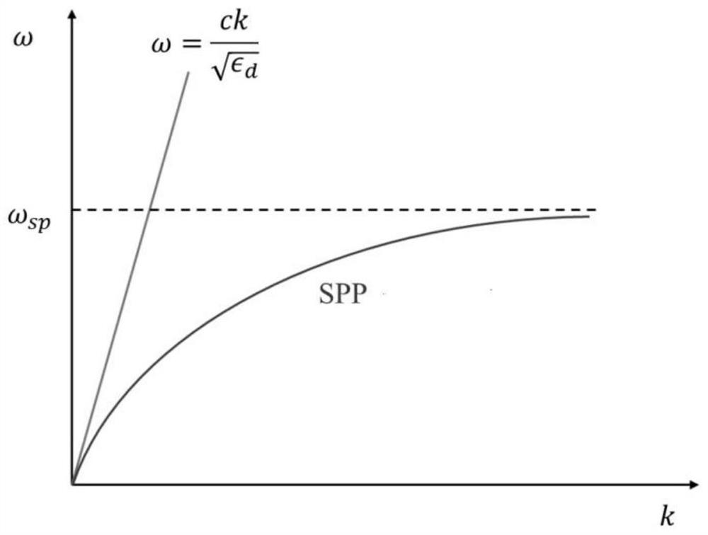
[0026] After in-depth research, it is found that the existing LV-SEM based on thermal emission, Schottky field emission, and cold field emission electron sources still have difficulties in achieving further breakthroughs in resolution, and the current research on photoelectron emission electron sources still has Optimize space.
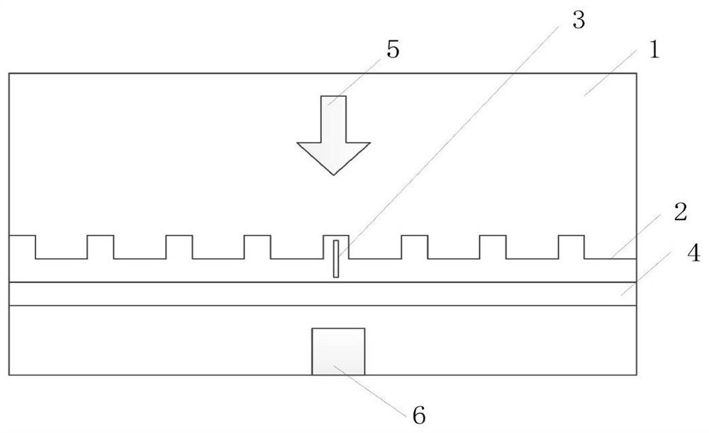
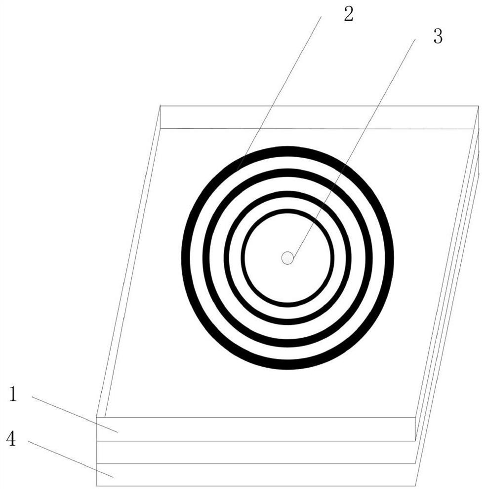
[0027] The elect...


PUM


Abstract

The embodiment of the invention provides a surface plasmon-induced electron emission source, which is characterized in that a pumping source emits light to interact with a metal bull eye optical grating to generate a surface plasmon near field, the light reaches a photocathode material layer through a central small hole and interacts with a photocathode material to generate electrons, an electroncollector collects the electrons, the period of the metal bull eye optical grating and the wave vector of the surface plasmon meet the condition that the cross product of the period of the metal bulleye optical grating and the wave vector of the surface plasmon is an integral multiple of 2pi, and the photocathode material layer is a preset special material, so that the surface plasmon near fieldirradiates the photocathode material to generate a photoinduced electron emission phenomenon. According to the embodiment of the invention, based on a high-resolution electron source combining a photoinduced electron emission principle and surface plasmon polaritons, the energy dissipation of electron beams is reduced, and the brightness is improved.

Description

technical field [0001] The invention relates to the field of electronic technology, in particular to an electron emission source induced by surface plasmons. Background technique [0002] In recent years, the development of microscopy instruments has made great progress, and one of the key advances is the Low Voltage-Scanning Electron Microscope (LV-SEM). Low-voltage scanning electron microscopes are a class of scanning electron microscopes with electron accelerating voltages below 10kV. The advantages of LV-SEM are: the energy and speed of the electron beam used are low, and the depth of the penetration into the sample is small, so the volume of the interaction area between the electron and the sample is reduced. This advantage can be used to detect surface sensitive information that cannot be obtained by traditional scanning electron microscopes; low The scanning electron microscope with the accelerating voltage can realize the scanning image with good contrast; reducing ...

Claims


Application Information

Patent Timeline
Patent Type & Authority Applications(China)
IPC IPC(8): H01J1/34H01J37/26H01J37/28H01J40/06
CPCH01J1/34H01J37/26H01J37/28H01J40/06
Inventor 刘仿王哲宣黄翊东崔开宇冯雪张巍
Owner TSINGHUA UNIV
Why Eureka
Try Eureka