Parameter optimization design method for SiC MOSFET (Metal-Oxide-Semiconductor Field Effect Transistor) driving circuit

A technology for optimizing design and driving circuits, applied in CAD circuit design, design optimization/simulation, special data processing applications, etc., can solve the problems that the key stray parameters of SiCMOSFET have not been considered, and the optimal design method of SiCMOSFET driving circuit parameters is not complete, etc. Achieve the effects of improving design reliability, saving design time, and simple methods

Active Publication Date: 2021-03-05
BEIJING JIAOTONG UNIV +1
View PDF3 Cites 1 Cited by
  • Summary
  • Abstract
  • Description
  • Claims
  • Application Information

AI Technical Summary

Problems solved by technology

[0004] These studies have explained the essential cause of gate-source voltage interference, and provided a conceptual basis for improving gate drive circuit design, eliminating interference, and increasing switching speed; however, these studies have not yet considered the key stray parameters that affect the dynamic characteristics of SiC MOSFETs, such as Gate internal resistance, drive loop inductance and power loop inductance, etc.
The optimization design method of SiC MOSFET drive circuit parameters is not yet complete, and it is urgent to explore the drive design method suitable for SiC MOSFET based on the characteristics of high switching speed of SiC MOSFET, so as to provide SiC MOSFET devices with higher power level and higher performance requirements in the future. Provide theoretical guidance and application technical support

Method used


Image

  • Parameter optimization design method for SiC MOSFET (Metal-Oxide-Semiconductor Field Effect Transistor) driving circuit
  • Parameter optimization design method for SiC MOSFET (Metal-Oxide-Semiconductor Field Effect Transistor) driving circuit
  • Parameter optimization design method for SiC MOSFET (Metal-Oxide-Semiconductor Field Effect Transistor) driving circuit

Examples


Embodiment Construction

[0056] An embodiment of the present invention:

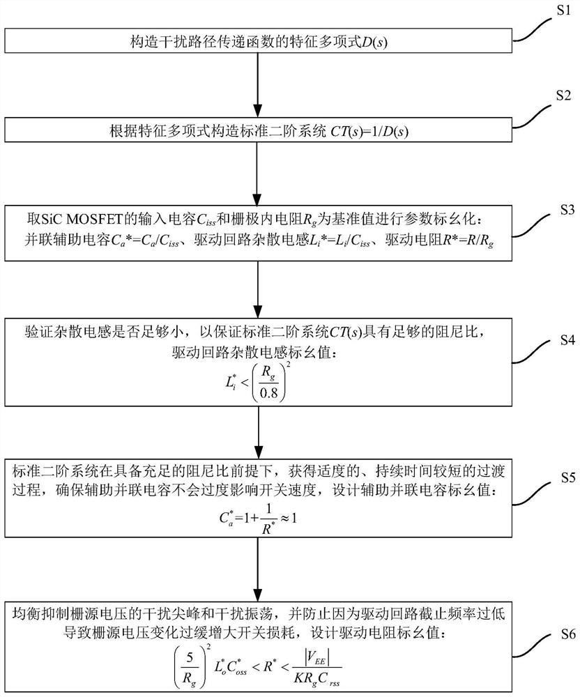
[0057] Such as figure 1 As shown, the method includes the following steps:

[0058] Step S1: Construct the characteristic polynomial D(s) of the interference path transfer function;

[0059] Step S2: Construct a standard second-order system CT(s)=1 / D(s) according to the characteristic polynomial;

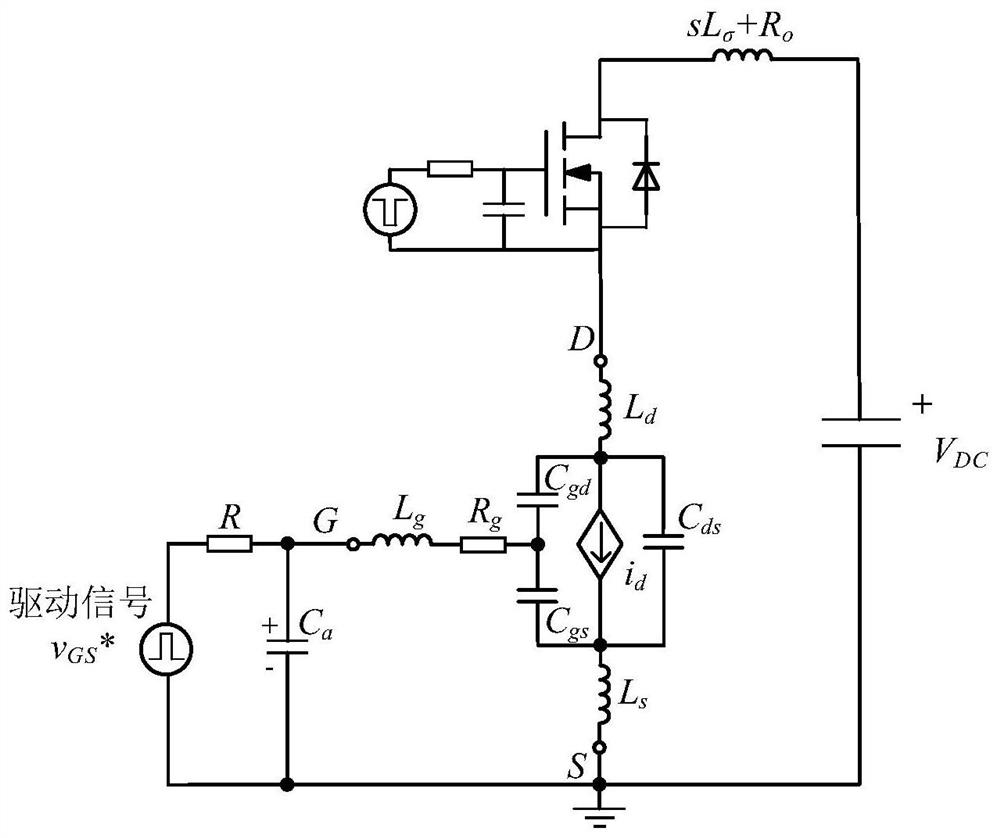
[0060] Step S3: Take the input capacitance C of the SiC MOSFET iss and gate internal resistance R g Parametric Unitization for Reference Values: Parallel Auxiliary Capacitor Drive circuit stray inductance Drive resistor R * =R / R g ;

[0061] Step S4: Verify whether the stray inductance is small enough to ensure that the standard second-order system CT(s) has a sufficient damping ratio, and the per unit value of the stray inductance of the drive circuit is:

[0062]

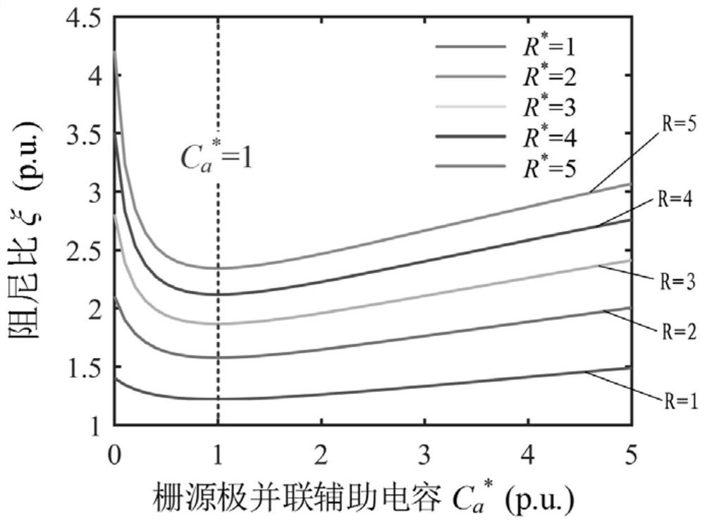
[0063] Step S5: Under the premise of sufficient damping ratio, the standard second-order system obtains a moderate transition process with a short duration ...


PUM


Abstract

The invention provides a SiC MOSFET driving circuit parameter optimization design method, which is used for improving the design reliability of a SiC-based power electronic converter. The parameter design method comprises the following steps: constructing a characteristic polynomial of an interference path transfer function; constructing a standard second-order system according to the characteristic polynomial; taking the input capacitance Ciss of the SiC MOSFET and the resistance Rg in the grid electrode as reference values to carry out parameter per-unit; and verifying whether the stray inductance is small enough or not so as to ensure that the standard second-order system has an enough damping ratio; an auxiliary parallel capacitor per-unit value is designed, so that the standard second-order system obtains a proper transition process with short duration on the premise of having a sufficient damping ratio, and it is ensured that the auxiliary parallel capacitor does not excessivelyinfluence the switching speed; the per-unit value of the driving resistor is designed, the interference peak and interference oscillation of the gate-source voltage are suppressed in a balanced manner, and the switching loss is prevented from being increased due to too slow gate-source voltage change caused by too low cut-off frequency of a driving loop.

Description

technical field [0001] The invention relates to a parameter optimization design method of a SiC MOSFET driving circuit. Background technique [0002] At present, in practical application of SiC MOSFET, the drive design method of traditional SiC MOSFET is still used. However, SiC MOSFETs generally have faster switching speeds and higher voltage withstand capabilities, so they have a higher voltage change rate than Si devices, and the gate-source voltage interference problem is more prominent. [0003] The two main factors that limit the switching speed of their SiC MOSFETs are gate drive capability and gate-source voltage interference issues. Reference [1], Reference [2] and Reference [3], on the basis of traditional SiMOSFET drive circuit design, additionally add the verification link of the maximum change value of gate-source voltage, according to the voltage change rate, drive resistance and junction capacitance, etc. The effective circuit estimates the maximum change va...

Claims


Application Information

Patent Timeline
Patent Type & Authority Applications(China)
IPC IPC(8): G06F30/20G06F30/30
CPCG06F30/20G06F30/30
Inventor 邵天骢郑琼林李志君李虹黄波邱志东张志朋王作兴王佳信
Owner BEIJING JIAOTONG UNIV
Why Eureka
Try Eureka