

Double-sided laminated airtight brazing system and method in 3D microwave radio frequency module
A microwave radio frequency, 3D technology, applied in welding equipment, auxiliary devices, manufacturing tools, etc., can solve the problems of energy waste, low efficiency, complex welding process, etc. Effect
- Summary
- Abstract
- Description
- Claims
- Application Information
AI Technical Summary
Problems solved by technology
Method used
Image

Examples
Embodiment 1
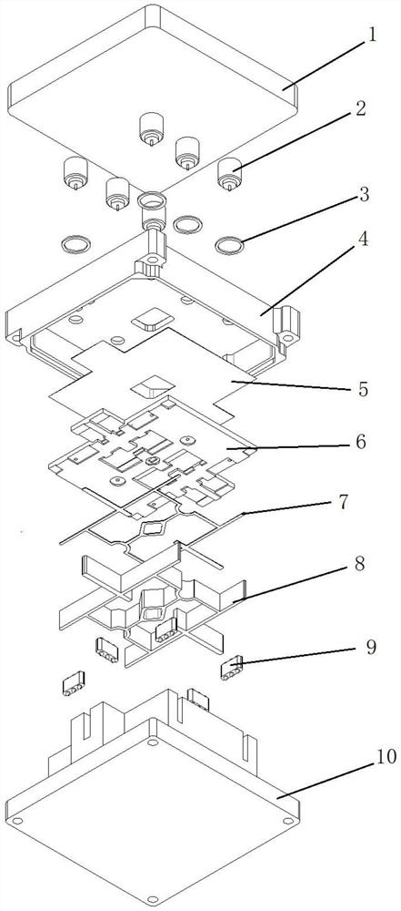
[0029] Such as figure 1 as shown, figure 1 It is a structural exploded view of the double-sided laminated airtight brazing system in the 3D microwave radio frequency module; the double-sided laminated airtight brazing system in the 3D microwave radio frequency module of the present invention includes an upper tooling 1, a connector 2, a connecting Device solder ring 3, module shell 4, substrate solder 5, substrate 6, surface device solder 7, surface device 8, elastic tooling 9, and lower tooling 10. The connector 2 and the connector solder ring 3 are arranged between the upper tooling 1 and the module shell 4, the substrate solder 5, the substrate 6, the surface component solder 7, the The surface device 8 and the elastic tooling 9 are arranged between the lower tooling 10 and the module shell 4 .
[0030] Specifically, the lower end surface of the module shell 4 is provided with a concave cavity, and the cavity is sequentially provided with the substrate solder 5, the subst...
Embodiment 2
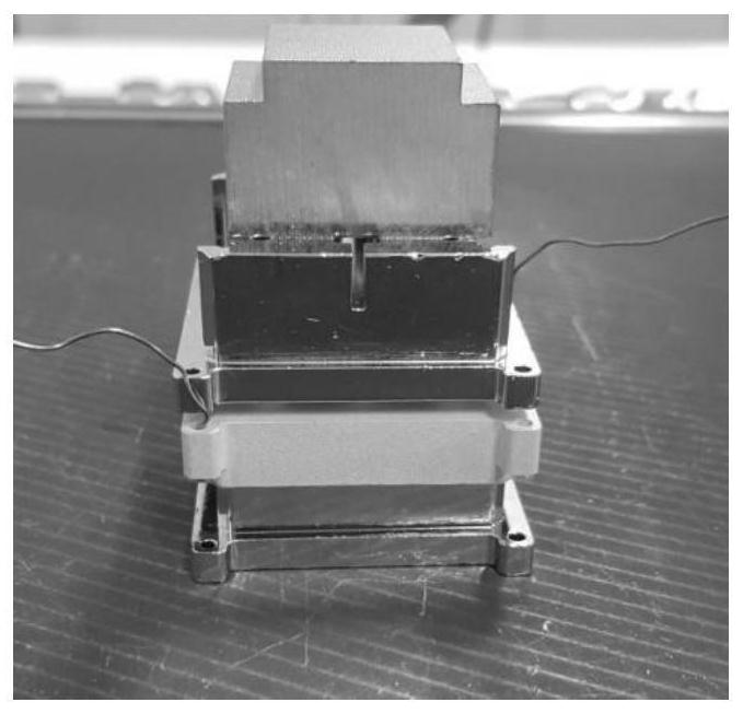
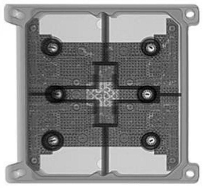
[0039] Such as figure 2 , image 3 as shown, figure 2 It is the actual welding schematic diagram of the double-sided laminated airtight brazing method in the 3D microwave radio frequency module; image 3 It is the X-ray inspection diagram of the assembly after welding by the double-sided laminated airtight brazing method in the 3D microwave radio frequency module; the brazing method of the double-sided laminated airtight brazing system in the 3D microwave radio frequency module of the present invention, according to Follow the steps below:
[0040] S1, placing the cavity of the module shell 4 facing upwards on a flat surface;
[0041] S2, sequentially place the substrate solder 5, the substrate 6, the surface device solder 7, the surface device 8, the elastic tooling 9 and the lower tooling 10 into the cavity of the module shell 4 ;
[0042]S3, the substrate solder 5, the substrate 6, the surface device solder 7, the surface device 8, the elastic tooling 9, the lower to...
PUM
 Abstract
Description
Claims
Application Information