Switching type broadband terahertz wave absorber based on VO2 and absorption device

A terahertz and wave absorption technology, applied in the field of terahertz waves, can solve the problems of low absorption rate, no broadband absorption effect, and inability to turn off the terahertz wave absorption function of the terahertz absorber well, and achieve wide absorption characteristics , The effect of low design and preparation difficulty and simple structure

Pending Publication Date: 2021-03-12
YUNNAN NORMAL UNIV
View PDF9 Cites 0 Cited by
  • Summary
  • Abstract
  • Description
  • Claims
  • Application Information

AI Technical Summary

Problems solved by technology

Among them, the vanadium dioxide phase-change layer is in the form of a thin film and is used as a reflective layer; however, the terahertz wave absorber has two narrow-band absorption peaks when the vanadium dioxide is in the metal phase, and does not have a broadband absorption effect, and The absorption rate of one of the absorption peaks is low, less than 60%; in addition, the absorption rate of the terahertz wave absorber in the range of 2THz to 3THz will gradually increase from 0% to more than 20% when the vanadium dioxide is in the insulating phase , cannot close the terahertz wave absorption function of the terahertz absorber very well

Method used


Image

  • Switching type broadband terahertz wave absorber based on VO2 and absorption device
  • Switching type broadband terahertz wave absorber based on VO2 and absorption device
  • Switching type broadband terahertz wave absorber based on VO2 and absorption device

Examples


Embodiment Construction

[0034] The present invention will be described in further detail below in conjunction with specific examples, but the embodiments of the present invention are not limited thereto.

[0035] In order to improve the absorption bandwidth and absorption rate of the switch-type terahertz wave absorber without increasing the design and fabrication difficulty of the switch-type terahertz wave absorber, the embodiment of the present invention provides a VO-based 2 A switch-type broadband terahertz wave absorber and absorbing device.

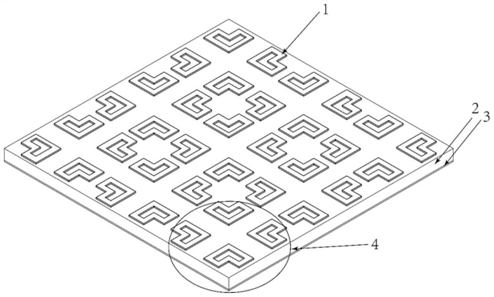
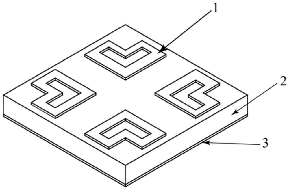
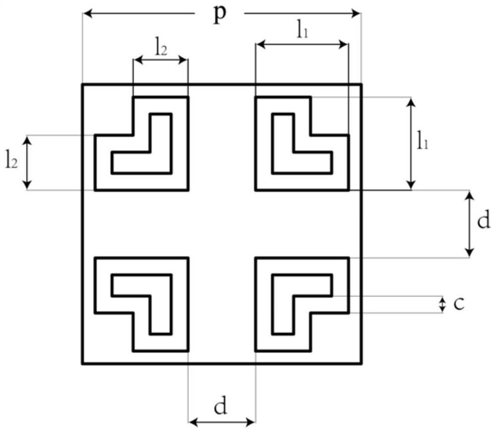
[0036] First of all, based on the VO provided by the embodiment of the present invention 2 The switch-type broadband terahertz wave absorber is described in detail. see figure 1 with figure 2 As shown, the switch-type broadband terahertz wave absorber includes: a plurality of microstructure units 4 arranged in a matrix.

[0037] Wherein, each microstructure unit 4 includes: a phase change material layer 1 , a medium layer 2 and a reflective layer 3 ;...


PUM

PropertyMeasurementUnit
lengthaaaaaaaaaa
widthaaaaaaaaaa
thicknessaaaaaaaaaa

Abstract

The invention discloses a switching type broadband terahertz wave absorber based on VO2. The switching type broadband terahertz wave absorber comprises a plurality of microstructure units arranged ina matrix form; each microstructure unit comprises a phase change material layer, a dielectric layer and a reflecting layer; the phase change material layer is located on the upper surface of the dielectric layer, and the reflecting layer is located on the lower surface of the dielectric layer; the phase change material layer comprises four L-shaped VO2 patches arranged in a matrix form; the middleof the L-shaped VO2 patch is hollowed out, and a hollowed-out pattern is in an L shape which is shrunk in proportion; wherein two long arms of each L-shaped VO2 patch extend towards the edge direction of the phase change material layer, and any two adjacent L-shaped VO2 patches are in mirror symmetry. The absorption bandwidth and the absorption rate of the switch type terahertz wave absorber canbe improved, and the design and preparation difficulty of the switch type terahertz wave absorber is not increased.

Description

technical field [0001] The invention belongs to the field of terahertz wave technology, in particular to a VO-based 2 A switch-type broadband terahertz wave absorber and absorbing device. Background technique [0002] The wave band of terahertz wave is between the millimeter wave band and the far-infrared wave band. Specifically, it refers to electromagnetic waves with a frequency of 0.1 THz to 10 THz and a wavelength of 0.03 mm to 3 mm. It belongs to the transitional research field from macroelectronics to microphotonics. Terahertz waves have unique transient properties, low energy, high penetration and anti-interference ability, and have broad application prospects in many fields such as wireless communication, biomedicine, imaging and sensors. Terahertz wave absorbers can be used for sensing, detection, and regulation of terahertz waves, and play a very important role in the application of terahertz technology. Among them, the terahertz wave absorber is mainly composed ...

Claims


Application Information

Patent Timeline
Patent Type & Authority Applications(China)
IPC IPC(8): H01Q17/00H01Q15/14
CPCH01Q17/007H01Q15/14
Inventor 王伟吴晓婷刘驰何瑞李育政
Owner YUNNAN NORMAL UNIV
Why Eureka
Try Eureka