Wafer edge polishing equipment and method

An edge and wafer technology, applied in the field of wafer edge polishing equipment, can solve the problems of low manual cleaning efficiency, equipment output rate drop, and labor cost increase, so as to avoid damage and chuck contamination, reduce labor costs, The effect of improving cleanliness

Inactive Publication Date: 2021-03-16
ZING SEMICON CORP
View PDF8 Cites 0 Cited by
  • Summary
  • Abstract
  • Description
  • Claims
  • Application Information

AI Technical Summary

Problems solved by technology

[0005] In view of the shortcomings of the prior art described above, the object of the present invention is to provide a wafer edge polishing equipment and method, which is used to solve the need for manual cleaning of existing wafer polishing equipment, and the particles in the polishing liquid accumulate on the polishing pad. and on the chuck, causing damage to the polishing pad and contamination of the chuck, and is likely to cause damage to the wafer; manual cleaning is inefficient, leading to problems such as an increase in labor costs and a decrease in equipment output.

Method used


Image

  • Wafer edge polishing equipment and method
  • Wafer edge polishing equipment and method
  • Wafer edge polishing equipment and method

Examples


Embodiment Construction

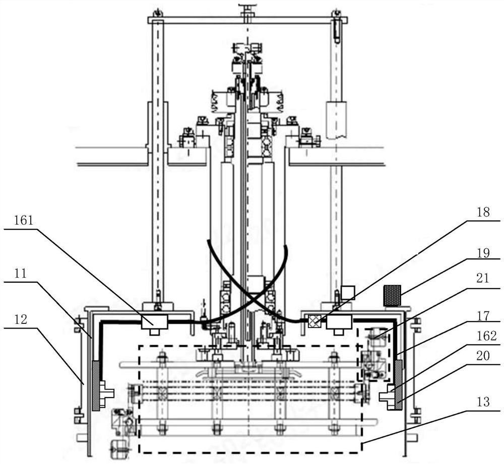
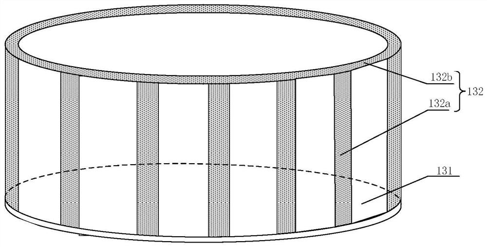
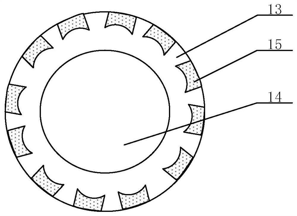
[0036] The implementation of the present invention will be illustrated by specific specific examples below, and those skilled in the art can easily understand other advantages and effects of the present invention from the contents disclosed in this specification.

[0037] see Figure 1 to Figure 3 . It should be noted that the structures, proportions, sizes, etc. shown in the drawings attached to this specification are only used to match the content disclosed in the specification, for those who are familiar with this technology to understand and read, and are not used to limit the implementation of the present invention. Limiting conditions, so there is no technical substantive meaning, any modification of structure, change of proportional relationship or adjustment of size, without affecting the effect and purpose of the present invention, should still fall within the scope of the present invention. within the scope covered by the disclosed technical content. At the same ti...


PUM


Abstract

The invention provides wafer edge polishing equipment and method. The equipment comprises a cavity, a sealing cover, a chuck, a carrying table, polishing pads, a cleaning device and a controller. Thesealing cover can move up and down to close or open the cavity; the chuck is located in the cavity and comprises a base and an annular side wall; the carrying table is located on the base; the polishing pads are located on the annular side wall of the chuck and distributed at the inner side of the annular side wall at intervals; the cleaning device comprises a nozzle and a cleaning pipeline, the nozzle is located in the cavity, one end of the cleaning pipeline is connected with a cleaning source, the other end of the cleaning pipeline is connected with the nozzle, and an automatic control valve is arranged on the cleaning pipeline; and the controller is connected with the automatic control valve and used for controlling the cleaning device to clean the chuck and the polishing pads after the edge polishing process is finished. By means of the wafer edge polishing equipment and method, particles in a polishing solution can be prevented from being accumulated on the equipment, damage to the polishing pads and pollution to the chuck are avoided, damage to wafers is avoided, the polishing yield and the equipment output rate can be increased, and the labor cost is reduced.

Description

technical field [0001] The invention relates to the technical field of wafer preparation, in particular to a wafer edge polishing device and method. Background technique [0002] Bare wafer (bare wafer) is one of the most basic and important raw materials in the semiconductor chip manufacturing process. Its manufacturing process usually includes pulling polysilicon material into high-quality The crystal pulling step of the single crystal silicon rod, the division of the single crystal silicon rod into multi-segment single crystal silicon rods, the grinding of the outer diameter of the single crystal silicon rod and the rolling and segmentation step of processing the notch (notch) at the same time, the single crystal silicon rod A dicing step for dividing into wafers, a step for improving the flatness of the wafer surface by grinding, etc. are performed. [0003] With the development of semiconductor manufacturing technology, the feature size of devices is shrinking and the ...

Claims


Application Information

Patent Timeline
IPC IPC(8): B24B37/00B24B37/11B24B37/27B24B37/34B24B55/00B24B57/02B24B53/017B08B3/02H01L21/67H01L21/304
CPCB24B37/00B24B37/11B24B37/27B24B37/34B24B55/00B24B57/02B24B53/017B08B3/02H01L21/67092H01L21/304
Inventor 吴祖安冯传浩浦兴东胡建平
Owner ZING SEMICON CORP
Why Eureka
Try Eureka