P-type gate enhanced GaN-based HEMT device and preparation method thereof
An enhanced, device technology, used in semiconductor/solid-state device manufacturing, semiconductor devices, electrical components, etc., can solve problems such as deteriorating device performance and reliability, improve performance and reliability, increase ionization efficiency, and reduce load. The effect of carrier traps and leakage channels
- Summary
- Abstract
- Description
- Claims
- Application Information
AI Technical Summary
Problems solved by technology
Method used
Image

Examples
Embodiment 1
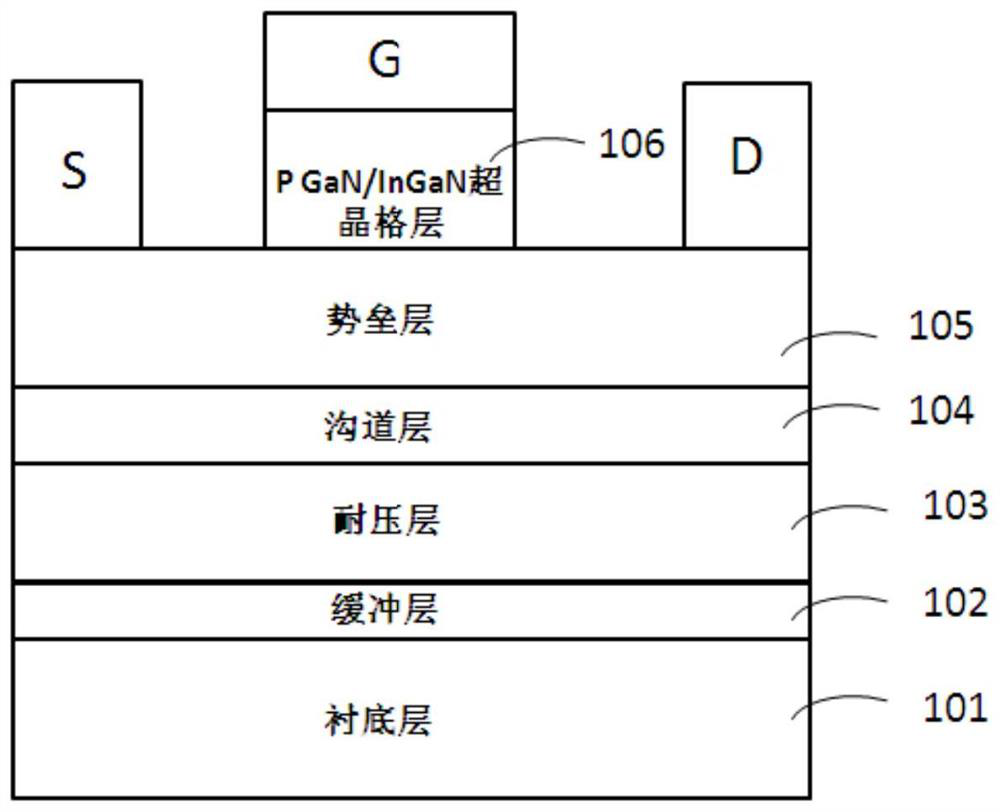
[0029] Prepared by the following steps as figure 1 The p-type gate-enhanced GaN-based HEMT device shown:
[0030]First, put the SiC substrate 101 into the MOCVD reaction chamber; then, grow a 200nm AlN buffer layer 102 at a pressure of 70torr and a temperature of 1000°C; 3000nm carbon-doped high-resistance GaN withstand voltage film layer 103; again change the growth conditions to 200torr pressure, 1050°C GaN growth conditions, grow 300nm UGaN channel layer 104; further change the conditions to 100torr pressure, 1030°C AlGaN Growth condition, grow the AlGaN barrier layer 105 of 25% Al composition of 15nm; Afterwards, grow p-type GaN / InGaN superlattice layer 106 on the AlGaN barrier layer 105, the cycle number is 15loop, p-type in each cycle Both the thickness of the GaN layer and the InGaN layer are 2nm, and the hole concentration of the p-type GaN layer is 2E18, the growth conditions are 200torr GaN growth gas flow, and the temperature is 950°C. Finally, the source S, the d...
Embodiment 2
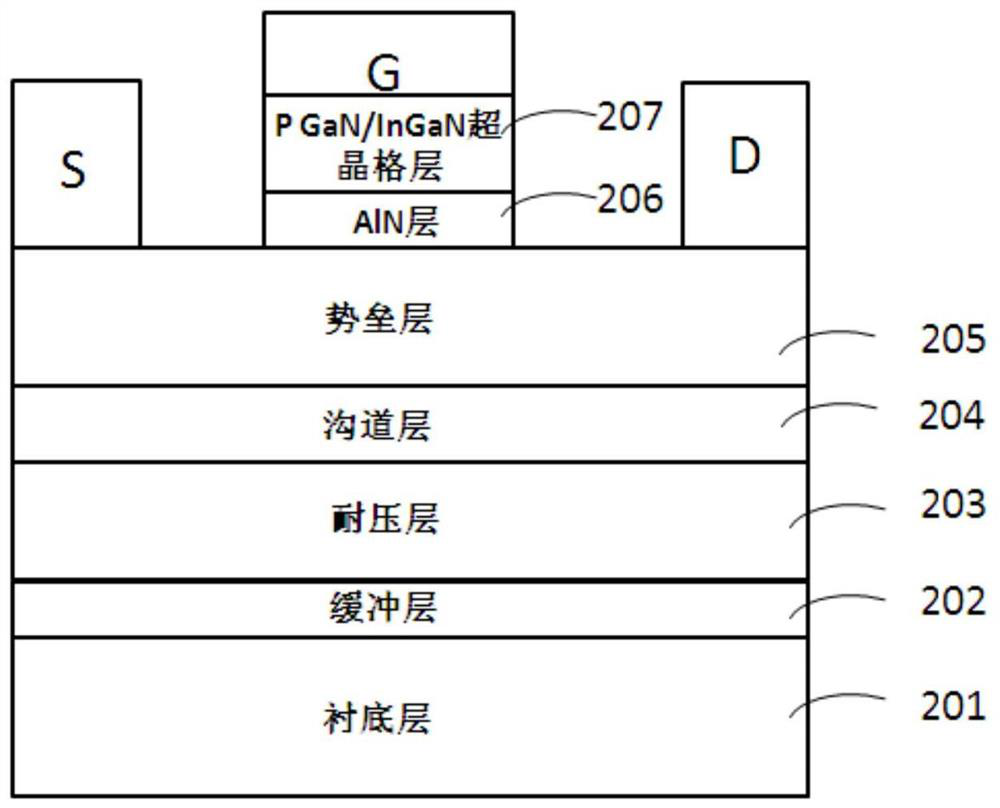
[0032] Prepared by the following steps as figure 2 The p-type gate-enhanced GaN-based HEMT device shown:
[0033] First, a silicon substrate 201 with a (111) crystal orientation is placed in an MOCVD reaction chamber, and the high-temperature H 2 treatment to remove surface oxides; then, grow a layer of 1000nm AlN / AlGaN multilayer buffer layer 202 at a pressure of 70torr and a temperature of 1000°C, wherein the thickness of the AlN layer is 300nm, and the thickness of the AlGaN layer is 700nm; change the atmosphere Under the GaN growth conditions of 70torr pressure and 1000°C, grow a 3000nm carbon-doped high-resistance gallium nitride withstand voltage film layer 203; change the growth conditions again to 200torr pressure, 1050°C GaN growth conditions, and grow a 300nm UGaN channel layer 204 ; change the conditions to 100torr pressure, AlGaN growth conditions at 1030°C, and grow a 15nm AlGaN barrier layer 205 with 25% Al composition; further change the growth conditions to 7...
PUM
| Property | Measurement | Unit |
|---|---|---|
| Thickness | aaaaa | aaaaa |
| Thickness | aaaaa | aaaaa |
| Thickness | aaaaa | aaaaa |
Abstract
Description
Claims
Application Information
 - R&D
- Intellectual Property
- Life Sciences
- Materials
- Tech Scout
- Unparalleled Data Quality
- Higher Quality Content
- 60% Fewer Hallucinations
Browse by: Latest US Patents, China's latest patents, Technical Efficacy Thesaurus, Application Domain, Technology Topic, Popular Technical Reports.
© 2025 PatSnap. All rights reserved.Legal|Privacy policy|Modern Slavery Act Transparency Statement|Sitemap|About US| Contact US: help@patsnap.com