

GaN-based semiconductor laser epitaxial structure and fabrication method thereof
A gallium nitride-based, epitaxial structure technology is applied in the structure of optical waveguide semiconductors, which can solve the problems of difficult to achieve high vertical conductivity and large sub-band hole quality, improve radiation compliance efficiency, enhance electron The effect of blocking and reducing loss
- Summary
- Abstract
- Description
- Claims
- Application Information
AI Technical Summary
Problems solved by technology
Method used
Image

Examples
Embodiment 1
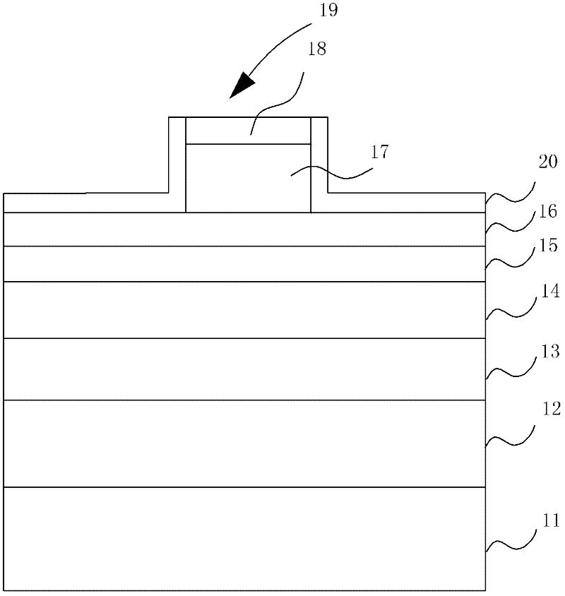
[0047] like figure 1 As shown, the epitaxial structure of the GaN-based semiconductor laser provided by the embodiment of the present invention includes:
[0048] The first layer is a gallium nitride substrate 11; wherein, the thickness of the gallium nitride substrate 11 is 300 μm, and Si is used as a donor impurity to form an n-type substrate, and its resistivity is about 0.001Ωcm.
[0049] The second layer is an n-type optical confinement layer 12; this layer is a periodic AlGaN / GaN material with a superlattice structure, wherein the thickness of the n-type optical confinement layer 12 is 2 μm, Si is used as a donor impurity, and the Al composition is 4 %.
[0050] The third layer is the optical waveguide layer 13 under n-type InGaN; wherein, the thickness of the optical waveguide layer 13 under n-type InGaN is 150 nm, the composition of In is 4%, and Si is used as the donor impurity, and its doping concentration is 1×10 17 cm -3 .
[0051] The fourth layer is ...
Embodiment 2
[0064] like figure 1 As shown, the epitaxial structure of the GaN-based semiconductor laser provided by the embodiment of the present invention includes:
[0065] The first layer is a SiC substrate 11; wherein, the thickness of the SiC substrate 11 is 300 μm, and Si is used as a donor impurity to form an n-type substrate, and its resistivity is about 0.001Ωcm.
[0066] The second layer is an n-type optical confinement layer 12; this layer is a periodic superlattice structure AlGaN / GaN material; wherein, the thickness of the n-type optical confinement layer 12 is 2 μm, Si is used as the donor impurity, and the Al composition is 4 %.
[0067] The third layer is the optical waveguide layer 13 under n-type GaN; wherein, the thickness of the optical waveguide layer 13 under n-type GaN is 150 nm, and Si is used as the donor impurity, and its doping concentration is 1×10 17 cm -3 .
[0068] The fourth layer is the multi-quantum well InGaN / GaN active region 14...
Embodiment 3
[0081] like figure 1 As shown, the epitaxial structure of the GaN-based semiconductor laser provided by the embodiment of the present invention includes:
[0082] The first layer is a SiC substrate 11; wherein, the thickness of the SiC substrate 11 is 300 μm, and Si is used as a donor impurity to form an n-type substrate, and its resistivity is about 0.001Ωcm.
[0083] The second layer is an n-type optical confinement layer 12; this layer is a periodic superlattice structure AlGaN / GaN material; wherein, the thickness of the n-type optical confinement layer 12 is 2 μm, Si is used as the donor impurity, and the Al composition is 4 %.
[0084] The third layer is the optical waveguide layer 13 under n-type InGaN; wherein, the thickness of the optical waveguide layer 13 under n-type InGaN is 150 nm, the composition of In is 8%, and Si is used as the donor impurity, and its doping concentration is 1×10 17 cm -3 .
[0085] The fourth layer is the multi-quantu...
PUM
| Property | Measurement | Unit |
|---|---|---|
| thickness | aaaaa | aaaaa |
| thickness | aaaaa | aaaaa |
| thickness | aaaaa | aaaaa |
Abstract
Description
Claims
Application Information