
Resistive random access memory structure and manufacturing method thereof

A technology of resistive random access and storage structure, which is applied in the direction of electrical components, etc., can solve the problems of poor product yield and reliability, holes in memory cells, and error-prone resistive random access storage devices, so as to improve yield and reliability, increasing the effect of complexity

Pending Publication Date: 2021-03-19
WINBOND ELECTRONICS CORP
View PDF8 Cites 0 Cited by
  • Summary
  • Abstract
  • Description
  • Claims
  • Application Information

AI Technical Summary

Problems solved by technology

When a low-k dielectric material is formed between a plurality of memory cells, due to the poor gap filling ability of the low-k dielectric material, holes will be generated between the plurality of memory cells
As a result, the operation of the resistive random access memory device is prone to errors, and the yield and reliability of the product are deteriorated

Method used


Image

  • Resistive random access memory structure and manufacturing method thereof
  • Resistive random access memory structure and manufacturing method thereof
  • Resistive random access memory structure and manufacturing method thereof

Examples


Embodiment Construction

[0027] The following will clearly and completely describe the technical solutions in the embodiments of the present invention with reference to the accompanying drawings in the embodiments of the present invention. Obviously, the described embodiments are only some, not all, embodiments of the present invention. Based on the embodiments of the present invention, all other embodiments obtained by persons of ordinary skill in the art without making creative efforts belong to the protection scope of the present invention.

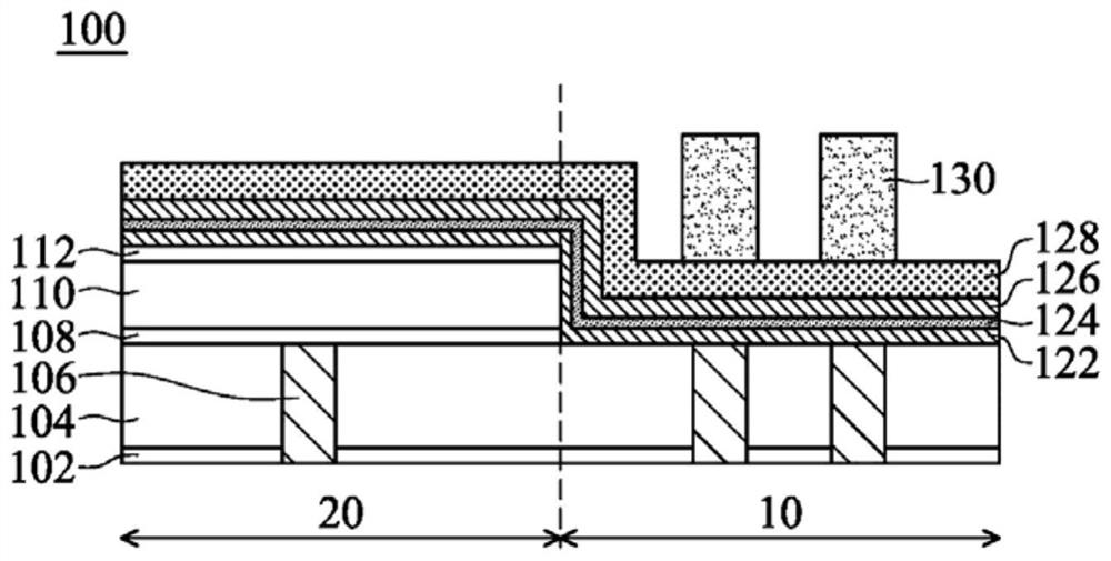
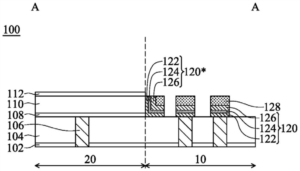
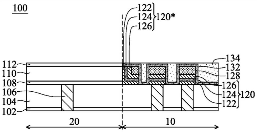
[0028] Please refer to Figure 1A , a substrate 102 is provided, and the substrate 102 includes an array region 10 and a peripheral region 20 surrounding the array region 10 . Next, an insulating layer 104 is formed on the substrate 102 . The insulating layer 104 can be, for example, silicon oxide. Next, a patterning process is performed on the insulating layer 104 to form openings. Next, metal material is filled into the opening to form a contact plug 106 ...


PUM


Abstract

The present invention provides a resistive random access memory structure and a manufacturing method thereof. The resistive random access memory structure comprises: a substrate having an array regionand a peripheral region; a first low-dielectric-constant dielectric layer, which is located in the peripheral area and has a dielectric constant of smaller than 3; a plurality of memory cells, whichare positioned on the substrate and are positioned in the array region; a gap filling dielectric layer, which is located in the array region, covers the memory cells and fills in space between the adjacent memory cells; a plurality of first conductive plugs, which are located in the gap filling dielectric layer, wherein each of the first conductive plugs is in contact with one of the memory cells;and a dummy memory unit, which is located at the junction of the array region and the peripheral region and is not in contact with any one of the first conductive plugs. According to the resistive random access memory structure provided by the invention, the yield and the reliability of a product can be obviously improved, and process complexity, production cost and production time are reduced.

Description

technical field [0001] The invention relates to a storage device, in particular to a resistive random access storage structure and a manufacturing method thereof. Background technique [0002] Resistive random access memory (RRAM) has the advantages of simple structure, small area, low operating voltage, fast operating speed, long memory time, multi-state memory, and low power consumption. Therefore, the resistive random access memory has great potential to replace the current flash memory and become the mainstream of the next generation non-volatile memory. [0003] In known RRAMs, a chip usually includes an array area and a peripheral area. The array area includes a plurality of memory cells, and each memory cell includes a patterned bottom electrode layer, a resistance transition layer and a top electrode layer. The peripheral area is mainly logic circuits. In the peripheral area, in order to increase the operating speed of the logic circuit, the dielectric layer uses ...

Claims


Application Information

Patent Timeline
Patent Type & Authority Applications(China)
IPC IPC(8): H01L45/00
CPCH10N70/801H10N70/841H10N70/011
Inventor 李彦德王景擁尤建祥陈宏生
Owner WINBOND ELECTRONICS CORP
Learn More