Secondary etching forming method for high-precision lead

A technology of secondary etching and forming method, which is applied in the direction of semiconductor devices, electrical components, circuits, etc. It can solve the problems of unable to check the tip area of ​​the lead, affect the quality of chip bonding, and the bonding force of the metal lead is small, so as to reduce the poor lead peeling Phenomenon, reduce missed detection, good etching effect

Pending Publication Date: 2021-03-23
LEADER TECH ELECTRONICS SHENZHEN INC
View PDF0 Cites 1 Cited by
  • Summary
  • Abstract
  • Description
  • Claims
  • Application Information

AI Technical Summary

Problems solved by technology

[0003] The existing high-precision lead processing steps have the following disadvantages: 1. The apex of the lead is corroded by the etching solution in three directions during etching, the apex becomes thinner, and the shape is needle-like, and the bonding area is reduced when bonding, which is easy to Causes weak soldering or insufficient soldering bonding force to affect the quality of chip bonding
2. Due to the thinning of the tip of the lead wire, the bonding pressure on the lead wire may occur during the chip bonding process, causing the lead wire to break and cause poor product functionality. The schematic diagram is as follows Figure 10 shown
3. Since the tip of the lead wire is thinner and has different shapes, it is impossible to check the tip area of ​​the lead wire during automatic optical inspection during the production process, which may cause missed inspection of defective products
4. As the wire width at the tip of the lead wire becomes smaller, the bonding force between the metal lead wire and PI becomes smaller. During the production and bonding process of COF products, the lead wire may be peeled off due to product curling or external force. The schematic diagram is as follows Figure 11 shown

Method used


Image

  • Secondary etching forming method for high-precision lead
  • Secondary etching forming method for high-precision lead
  • Secondary etching forming method for high-precision lead

Examples


Embodiment Construction

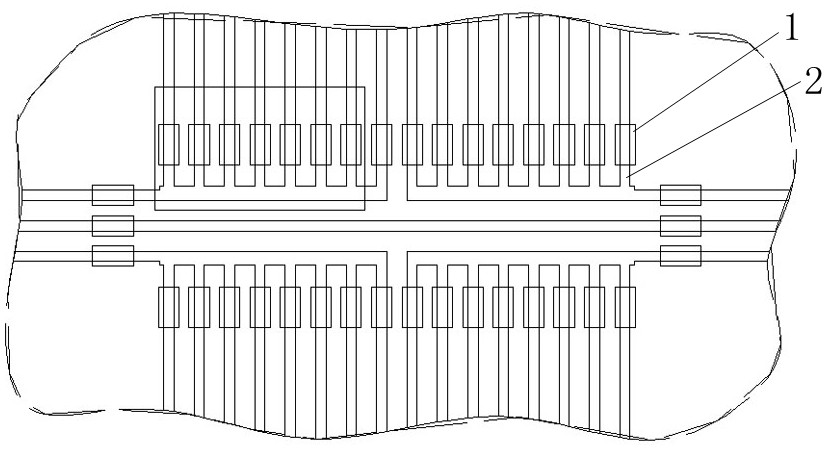
[0033] A high-precision lead secondary etching molding method is characterized in that a metal lead 2 is designed at the corresponding position of the chip pad 1 and connected to an external circuit, the overlapping area of ​​the chip pad 1 and the metal lead 2 is a bonding area, and the metal The tip of lead 2 exceeds the area of ​​chip pad 1 by a certain length, including steps:

[0034] Step A: If figure 1 As shown in the design stage, the metal lead 2 is directly connected to the internal circuit of the chip position on the product or the metal leads 2 on both sides of the chip are connected to each other so that there is no breakpoint at the tip of the metal lead 2 in the circuit. In the following steps, use figure 1 The box in is a description of the zoomed-in area;

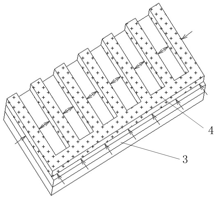
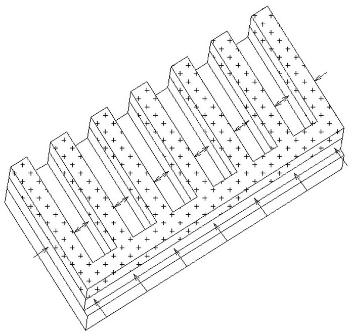
[0035] Step B: Coating a layer of photoresist 4 on the copper 3 of the product substrate, exposing the product substrate coated with photoresist 4, and using a developer to decompose the photoresist 4 at...


PUM


Abstract

The invention relates to a secondary etching forming method for a high-precision lead, and belongs to the technical field of high-precision circuit boards. In a design stage, leads on a high-precisioncircuit board are connected to an internal circuit at the position of a chip or leads on two sides of the chip are connected with each other; after a circuit is formed through primary etching, photoresist is applied again; secondary exposure is performed on the connection position of the leads; the photoresist at the secondary exposure position is developed; and secondary etching is performed, sothat a final lead shape is formed, and an ideal high-precision lead tip shape etching effect is obtained. According to the method, the etching positions are equal-interval line distances during primary etching, so that an etching effect is good; and when lead tips are formed during the secondary etching,the leads are only eroded by etching liquid in one direction, so that bonding pads have a larger bonding area during bonding, the bonding force of the leads and the bonding pads of the chip after welding is increased, the missing detection phenomenon of defective products is reduced, the product yield and reliability during bonding operation are improved, and the product yield and reliability are improved.

Description

technical field [0001] The invention relates to a high-precision lead wire secondary etching molding method, which belongs to the technical field of high-precision circuit boards. Background technique [0002] With the continuous improvement of chip processing capability requirements of electronic products in the market, packaged chips are rapidly developing towards high speed, integration, and miniaturization. The precision of the pads on the chip will continue to increase, and the precision of the leads on the corresponding COF products will need to be improved simultaneously. With the decrease of the lead width and line spacing, the impact of the potion on the erosion of the lead tip is more obvious when the line is etched, resulting in a decrease in the reliability of the packaged product and even a situation where the size of the lead tip cannot meet the packaging requirements. In order to solve the above problems and improve the etching precision of the lead tip, the ...

Claims


Application Information

Patent Timeline
Patent Type & Authority Applications(China)
IPC IPC(8): H01L21/48H01L21/60
CPCH01L24/43H01L21/4885H01L24/85H01L2224/43831
Inventor 戚胜利王健孙彬沈洪李晓华
Owner LEADER TECH ELECTRONICS SHENZHEN INC
Why Eureka
Try Eureka