Preparation method of multi-layer circuit board for 5G communication and multi-layer circuit board

A multi-layer circuit board and substrate technology, which is applied in multi-layer circuit manufacturing, printed circuit manufacturing, printed circuits connected with non-printed electrical components, etc., can solve the problem of limited space available for radiators, difficulty in dissipating heat, and heat conduction of PCB substrates Poor performance and other problems, to achieve the effect of high-density installation, improve heat dissipation effect, and improve heat conduction efficiency

Active Publication Date: 2021-03-26
JIAN MANKUN TECH
View PDF5 Cites 3 Cited by
  • Summary
  • Abstract
  • Description
  • Claims
  • Application Information

AI Technical Summary

Problems solved by technology

It is still difficult to dissipate excess heat due to the poor thermal conductivity of the PCB substrate and the limited space available for mounting the heat sink
[0004] With the advent of 5G, it has entered the era of miniaturization, high-density installation, and high-heating assembly. Due to the extensive use of surface mount components, a large amount of heat generated by components is transmitted to the PCB board. The low thermal conductivity of the PCB substrate will make It becomes quite difficult to remove excess heat from electronic systems
As a result, current state-of-the-art methods of removing excess heat from PCBs are less and less effective, hampering the longevity and stability of the board

Method used


Image

  • Preparation method of multi-layer circuit board for 5G communication and multi-layer circuit board
  • Preparation method of multi-layer circuit board for 5G communication and multi-layer circuit board
  • Preparation method of multi-layer circuit board for 5G communication and multi-layer circuit board

Examples


Embodiment Construction

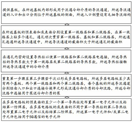
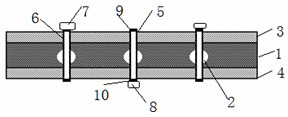
[0029] Specific embodiments of the present invention will be described in more detail below with reference to the accompanying drawings. Although specific embodiments of the invention are shown in the drawings, it should be understood that the invention may be embodied in various forms and is not limited to the embodiments set forth herein. Rather, these embodiments are provided for more thorough understanding of the present invention and to fully convey the scope of the present invention to those skilled in the art.

[0030] It should be noted that certain terms are used in the specification and claims to refer to specific components. Those skilled in the art should understand that they may use different terms to refer to the same component. The specification and claims do not use differences in nouns as a way of distinguishing components, but use differences in functions of components as a criterion for distinguishing. "Includes" or "comprises" mentioned throughout the spe...


PUM


Abstract

The invention discloses a preparation method of a multi-layer circuit board for 5G communication and the multi-layer circuit board. The preparation method comprises the steps that a substrate is provided, a flow guide channel used for circulating a cooling medium is formed in the substrate, a first circuit layer and a second circuit layer are arranged on the top surface and the bottom surface of the substrate respectively, a plurality of through holes are drilled in the first circuit layer, the through holes sequentially penetrate through the first circuit layer, the substrate and the second circuit layer, the through holes are communicated with the flow guide channel, heat conduction columns are arranged in the through holes in a sealed mode so as to enable the first circuit layer and thesecond circuit layer to be electrically connected, the heat conduction columns make contact with cooling media in the flow guide channels, the flow guide channels of all the substrates of the multilayer circuit board are connected with the condensation unit through inlets and outlets to form cooling flow paths for the cooling media to flow, a first electronic component is arranged and a first solder mask layer is adhered at at least one first heat conduction column on the top surface of the multilayer circuit board, and a second electronic component is arranged and a second solder mask layeris adhered at a second heat conduction column, different from the first heat conduction column, on the bottom surface of the multilayer circuit board.

Description

technical field [0001] The invention relates to the technical field of 5G communication circuit boards, in particular to a method for preparing a multilayer circuit board for 5G communication and a multilayer circuit board thereof. Background technique [0002] The fifth-generation mobile communication technology (5G) has higher speed and wider bandwidth. Its electronic components have more and more functions, and the packaging volume is getting smaller and smaller. Surface mount technology increases the installation density of electronic components. The effective heat dissipation area is reduced, but the processing capacity is getting stronger and stronger. The electronic components are bound to generate more heat during the working process, and the heat flux density is getting bigger and bigger, even reaching dozens to hundreds of W / cm 2 . If the heat is too high or the heat dissipation is not timely, it is easy to damage the electronic components, which requires the circ...

Claims


Application Information

Patent Timeline
Patent Type & Authority Applications(China)
IPC IPC(8): H05K1/02H05K1/18H05K3/46
CPCH05K1/0203H05K1/0204H05K1/181H05K3/4611H05K2201/06H05K2201/064
Inventor 肖学慧欧阳小军张孝斌
Owner JIAN MANKUN TECH
Why Eureka
Try Eureka