Packaging structure, preparation method thereof and photoelectric device
A packaging structure, optoelectronic device technology, applied in circuits, electrical components, electrical solid devices, etc., can solve the problems of poor device stability, water-oxygen isolation effect, poor thermal conductivity, short life, etc., to reduce interface thermal resistance, improve Water and oxygen barrier properties and the effect of improving thermal conductivity
- Summary
- Abstract
- Description
- Claims
- Application Information
AI Technical Summary
Problems solved by technology
Method used
Image

Examples
Embodiment 1
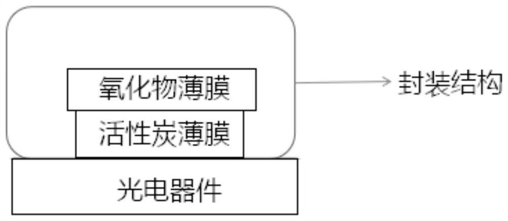
[0051] This embodiment provides an optoelectronic device. The optoelectronic device includes a substrate, a quantum dot light emitting diode combined on the substrate and a package structure for packaging the quantum dot light emitting diode. The structure of the photoelectric device is as follows from bottom to top: ITO substrate (50nm) / PEDOT:PSS (50nm) / poly-TPD (30nm) / quantum dot light-emitting layer (20nm) / ZnO (30nm) / Mg-Ag Alloy (50nm) / package structure (400mm).
[0052] On the ITO substrate, each layer is sequentially formed according to the quantum dot light emitting diode structure of this embodiment, thereby forming a quantum dot light emitting diode;
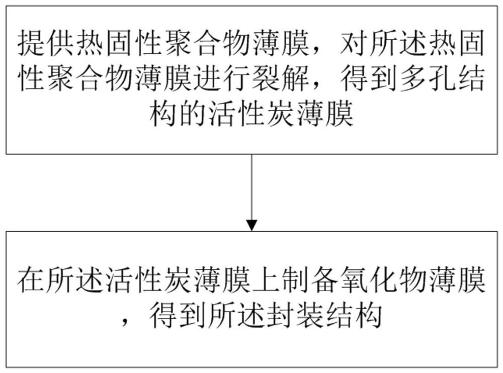
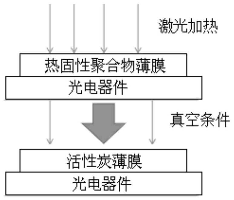
[0053] The encapsulation structure is composed of two layers: a 300nm thick porous activated carbon film, and a 100nm thick silicon dioxide film formed on the porous activated carbon film. The preparation process of the porous activated carbon film is as follows: make polyvinylidene chloride into ink, and then inkjet p...
Embodiment 2
[0056] This embodiment provides an optoelectronic device. The optoelectronic device includes a substrate, a quantum dot light emitting diode combined on the substrate and a package structure for packaging the quantum dot light emitting diode. The structure of the photoelectric device is as follows from bottom to top: ITO substrate (50nm) / PEDOT:PSS (50nm) / poly-TPD (30nm) / quantum dot light-emitting layer (20nm) / ZnO (30nm) / Mg-Ag Alloy (50nm) / package structure (600mm).
[0057] On the ITO substrate, each layer is sequentially formed according to the quantum dot light emitting diode structure of this embodiment, thereby forming a quantum dot light emitting diode;
[0058]The encapsulation structure is composed of two layers: a 300nm thick porous activated carbon film, and a 100nm thick silicon dioxide film formed on the porous activated carbon film. The preparation process of the porous activated carbon film is as follows: make polyacrylonitrile into ink, and then inkjet print it...
Embodiment 3
[0061] This embodiment provides an optoelectronic device. The optoelectronic device includes a substrate, a quantum dot light emitting diode combined on the substrate and a package structure for packaging the quantum dot light emitting diode. The structure of the photoelectric device is as follows from bottom to top: ITO substrate (50nm) / PEDOT:PSS (50nm) / poly-TPD (30nm) / quantum dot light-emitting layer (20nm) / ZnO (30nm) / Mg-Ag Alloy (50nm) / package structure (400mm).
[0062] On the ITO substrate, each layer is sequentially formed according to the quantum dot light emitting diode structure of this embodiment, thereby forming a quantum dot light emitting diode;
[0063] The encapsulation structure consists of two layers: a 300nm thick porous activated carbon film, and a 100nm thick titanium dioxide film formed on the porous activated carbon film. The preparation process of the porous activated carbon film is as follows: polyvinylidene chloride compound Ink, then inkjet printing...
PUM
| Property | Measurement | Unit |
|---|---|---|
| diameter | aaaaa | aaaaa |
| thickness | aaaaa | aaaaa |
| thickness | aaaaa | aaaaa |
Abstract
Description
Claims
Application Information
 - R&D
- Intellectual Property
- Life Sciences
- Materials
- Tech Scout
- Unparalleled Data Quality
- Higher Quality Content
- 60% Fewer Hallucinations
Browse by: Latest US Patents, China's latest patents, Technical Efficacy Thesaurus, Application Domain, Technology Topic, Popular Technical Reports.
© 2025 PatSnap. All rights reserved.Legal|Privacy policy|Modern Slavery Act Transparency Statement|Sitemap|About US| Contact US: help@patsnap.com