Voltage Adaptive Laser Driving Circuit and Its Control Method
A driving circuit and laser technology, applied in the direction of lasers, semiconductor lasers, laser components, etc., can solve the problem of non-adjustable power supply, the application of PWM pulse width modulation without considering the working efficiency of lasers, and the adjustment of laser voltage without realizing the laser PWM pulse width modulation and other issues
- Summary
- Abstract
- Description
- Claims
- Application Information
AI Technical Summary
Problems solved by technology
Method used
Image
Examples
Embodiment 1
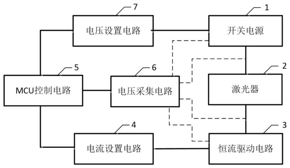
[0049] Such as figure 1 As shown, it is a block diagram for realizing the voltage adaptive laser driving circuit according to the embodiment of the present invention. It includes a switching power supply 1, a laser 2, a constant current drive circuit 3, a current setting circuit 4, an MCU control circuit 5, a voltage acquisition circuit 6, and a voltage setting circuit 7.
[0050] The switching power supply supplies power to the laser. There are many ways to realize the switching power supply. It can adopt a non-isolated topology or an isolated switching power supply topology. The characteristic of the switching power supply is that the external performance of the switching power supply should include input voltage VCC, output voltage OUT, Reset signal RESET, voltage adjustment pin FB.
[0051] The laser is an LD laser, or other types of lasers driven by constant current; the laser can also be in the form of an external terminal, and the user can connect to the desired laser ...
Embodiment 2
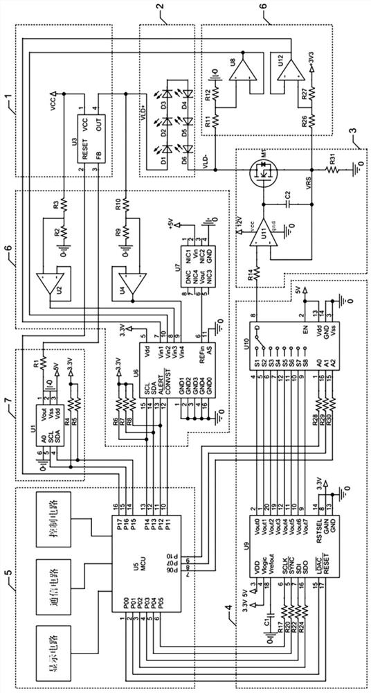
[0071] Such as image 3 As shown, it is a circuit diagram of the second implementation mode of the voltage adaptive laser drive circuit according to the embodiment of the present invention. The difference from Embodiment 1 is that the constant current drive circuit 3 is a current parallel negative feedback structure, the linear constant current power tube is M1, the current sampling resistor R31, and one end of the resistor R32 is connected to the negative input terminal of the op amp, and the other end is connected to the current sampling resistor The input terminal of R31, one end of resistor R14 is connected to the output signal of current setting circuit 4, the other end of resistor R14 is connected to the input negative pole of operational amplifier U11, the positive pole of operational amplifier U11 is connected to the output terminal of reference voltage chip U13, and the output terminal of operational amplifier U11 The signal is connected to the gate of the power MOS t...
Embodiment 3
[0075] Such as Figure 4 Shown is a block diagram of the internal implementation of the switching power supply according to the embodiment of the present invention. In Embodiment 1 or Embodiment 2, the MCU control circuit controls the voltage setting circuit and the output voltage of the switching power supply to be set, and the internal circuit diagram of the switching power supply is as follows Figure 4 As shown, the calculation formula of the open-loop setting of the output voltage at this time is:
[0076] Formula 3
[0077]In formula 3, Vout is the output voltage of the switching power supply; VT is the output voltage of the DA conversion circuit in the voltage setting circuit; VFB is the input voltage of the switching power supply circuit, which is the reference pin of the output voltage Vout, also called the output feedback pin , connected to the input terminal of the internal error amplifier to set the output voltage; K2 is the ratio of the resistor R13 to the re...
PUM
 Abstract
Description
Claims
Application Information


