Multilayer Broadband Metamaterial Absorber Based on Multimode Resistor and Design Method thereof

An absorber and metamaterial technology, applied in electrical components, antennas, etc., can solve the problem of thick broadband absorber thickness, and achieve the effect of easy processing, thin thickness, and superior broadband absorber performance.

Active Publication Date: 2022-06-28
AIR FORCE UNIV PLA
View PDF0 Cites 0 Cited by
  • Summary
  • Abstract
  • Description
  • Claims
  • Application Information

AI Technical Summary

Problems solved by technology

[0004] The purpose of the present invention is to propose a multi-layer broadband absorber based on multi-mode resistance and its design method to solve the problem that the thickness of the multi-layer structure is too thick to realize the broadband absorber

Method used


Image

  • Multilayer Broadband Metamaterial Absorber Based on Multimode Resistor and Design Method thereof
  • Multilayer Broadband Metamaterial Absorber Based on Multimode Resistor and Design Method thereof
  • Multilayer Broadband Metamaterial Absorber Based on Multimode Resistor and Design Method thereof

Examples


Embodiment Construction

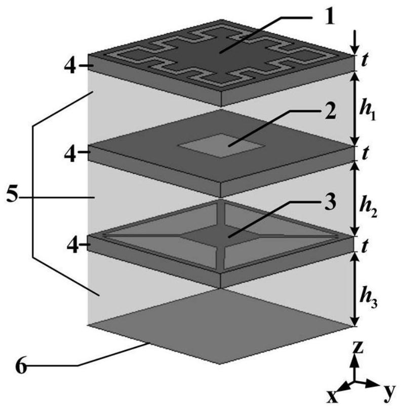
[0055] The technical solutions of the present invention are described in further detail below in conjunction with the accompanying drawings;

[0056] 1. Single-layer ITO structure design

[0057] In order to explain the wave absorption mechanism based on the multimode resistive wave absorber and lay the foundation for the later selection of the ITO structure type, the wave absorption characteristics of the single-layer ITO structure are characterized based on the simulation software CST Microwave Studio.

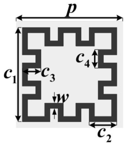
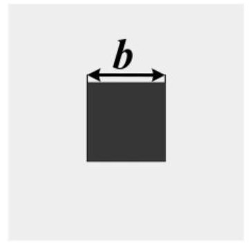
[0058] by Figure 4 Take the symmetrical four-trapezoid composite patch ITO structure as an example, first determine the influence of thickness and period on the absorbing performance. In order to distinguish it from the final multilayer absorbing body structure, here we use t 1 and p 1 represent the thickness and period of the monolayer ITO structure, respectively. like Figure 5 (a), with the thickness t 1 The increasing operating frequency band gradually moves toward...


PUM

PropertyMeasurementUnit
thicknessaaaaaaaaaa
electrical conductivityaaaaaaaaaa
thicknessaaaaaaaaaa

Abstract

The invention belongs to the technical field of metamaterial wave absorbing, in particular to a multi-layer broadband metamaterial wave absorber based on multimode resistance and a design method thereof. The metamaterial absorber of the present invention is an array formed by the periodic extension of the absorber unit along the x and y directions, and the period size is p; the absorber unit is composed of a bottom metal floor and three layers of absorber-dielectric plates stacked ; The absorbing layer is an ITO resistive film printed on a PET film; the top layer of the absorber unit is a circular meandering line ITO structure, the middle layer is a square patch structure, and the bottom layer is a symmetrical four-trapezoidal combination patch structure; The two layers of PET films are separated by a dielectric plate; the bottom of the unit is a metal floor; the unit structure is centrally symmetrical; the present invention determines the structural parameters of the absorber unit by optimizing the design, so that the metamaterial absorber is excited by TE and TM polarized waves Both of them show excellent broadband absorbing performance, and have angle insensitivity under TM polarization; the thickness is small, the structure is simple, and the processing is convenient.

Description

technical field [0001] The invention belongs to the technical field of metamaterial wave absorption, and specifically designs a multi-layer broadband metamaterial wave absorber based on multimode resistance and a design method thereof. Background technique [0002] The modern warfare environment has become more and more complex, and the requirements for the stealth performance and electromagnetic compatibility of weapons and equipment on the battlefield are also increasing. Traditional radar absorbing materials have been difficult to meet the requirements of "thin, light, wide and strong". With the development of science and technology, in the application scenario of the Internet of Everything, the problems of multi-antenna interference, electromagnetic radiation and pollution are becoming more and more serious. Metamaterial wave-absorbing technology can not only provide solutions for stealth technology and electromagnetic compatibility, but also suppress electromagnetic rad...

Claims


Application Information

Patent Timeline
Patent Type & Authority Patents(China)
IPC IPC(8): H01Q17/00
CPCH01Q17/008
Inventor 许河秀王彦朝王朝辉逄智超徐健徐硕
Owner AIR FORCE UNIV PLA
Why Eureka
Try Eureka