Memory structure and forming method thereof

A memory and storage gate technology, applied in the direction of electric solid state devices, semiconductor devices, electrical components, etc., can solve the problem of NAND memory structure performance needs to be improved, and achieve the effect of increasing the surface area, avoiding accumulation, and reducing material accumulation.

Pending Publication Date: 2021-04-16
SEMICON MFG INT (SHANGHAI) CORP +1
View PDF0 Cites 0 Cited by
  • Summary
  • Abstract
  • Description
  • Claims
  • Application Information

AI Technical Summary

Problems solved by technology

[0004] However, the performance of the NAND memory str

Method used


Image

  • Memory structure and forming method thereof
  • Memory structure and forming method thereof
  • Memory structure and forming method thereof

Examples


Embodiment Construction

[0036] As mentioned in the background, the performance of the memory structure formed in the prior art still needs to be improved. The following will describe in detail in conjunction with the accompanying drawings.

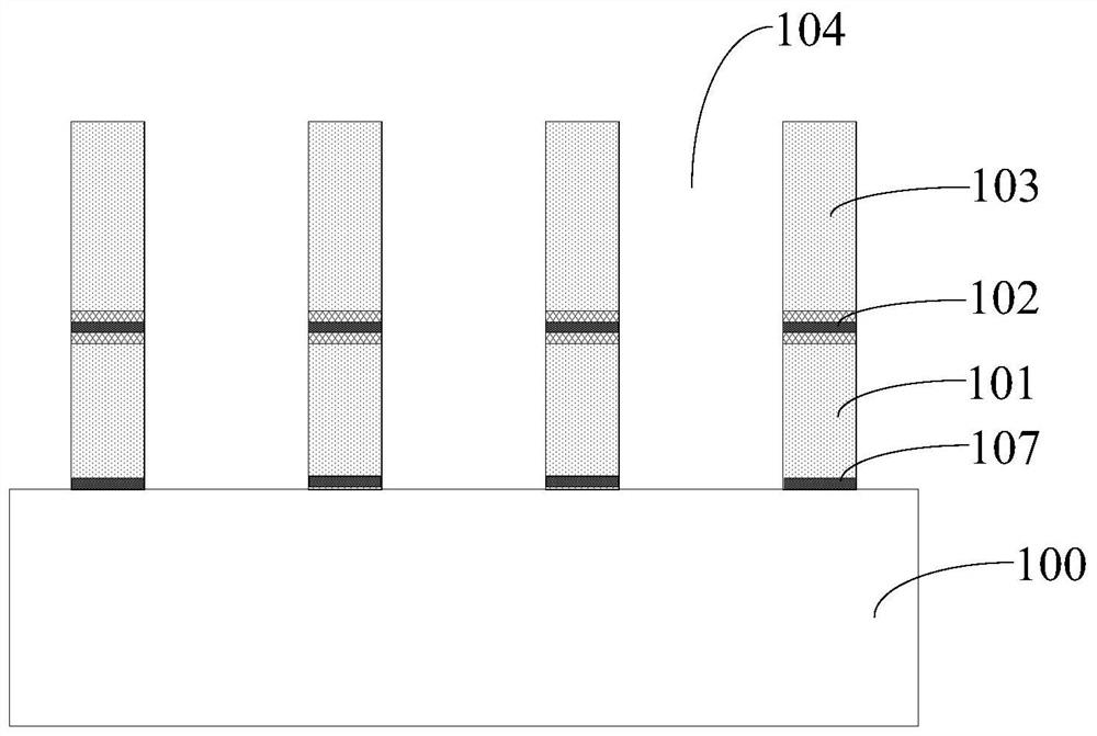
[0037] Please refer to figure 1 , providing a substrate 100, on which a plurality of separate storage gate structures are formed, with isolation grooves 104 between adjacent storage gate structures, and the storage structure includes a first gate dielectric layer 107, The floating gate layer 101 on the first gate dielectric layer 107 , the second gate dielectric layer 102 on the floating gate layer 101 , and the control gate layer 103 on the second gate dielectric layer 102 .

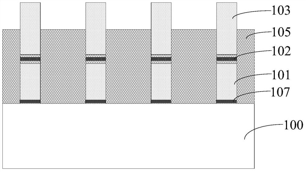
[0038] Please refer to figure 2 , forming an isolation layer 105 in the isolation groove 101, the top surface of the isolation layer 105 is lower than the top surface of the control gate layer 103, and the top surface of the isolation layer 105 is higher than that of the control gate l...


PUM

PropertyMeasurementUnit
Thicknessaaaaaaaaaa

Abstract

The invention discloses a memory structure and a forming method thereof. The forming method comprises the steps of providing a substrate; forming a plurality of storage gate structures which are separated from one another on the substrate, forming an isolation groove between adjacent storage gate structures, and enabling each storage gate structure to comprise a floating gate layer and a control gate layer located on the floating gate layer; forming an isolation layer in the isolation groove, wherein the top surface of the isolation layer is lower than the top surface of the control gate layer, and the top surface of the isolation layer is higher than the bottom surface of the control gate layer; forming a notch in the exposed side wall of the control gate layer, wherein the bottom of the notch is lower than or flush with the top surface of the isolation layer; and forming an initial metal silicide layer on the exposed surface of the control gate layer and the top surface of the isolation layer. By forming the notch at the junction of the isolation layer and the control gate layer, the surface area of the junction is effectively increased, and the situation that the electrical property of the finally formed memory structure is affected due to the fact that sharp protrusions are formed in the subsequent annealing treatment because the material of the initial metal silicide layer is accumulated at the junction is avoided.

Description

technical field [0001] The invention relates to the technical field of semiconductor manufacturing, in particular to a memory structure and a forming method thereof. Background technique [0002] In recent years, the development of flash memory (flash memory) is particularly rapid. The main feature of flash memory is that it can keep stored information for a long time without power on. [0003] NAND flash memory is a better storage solution than hard disk drives. Since NAND flash memory reads and writes data in units of pages, it is suitable for storing continuous data, such as pictures, audio or other file data; at the same time because of its low cost and large capacity Moreover, the advantages of fast writing speed and short erasing time are widely used in the storage field of mobile communication devices and portable multimedia devices. [0004] However, the performance of the NAND memory structure formed in the prior art still needs to be improved. Contents of the in...

Claims


Application Information

Patent Timeline
IPC IPC(8): H01L27/11524H01L21/28H01L29/423
CPCH01L29/40114H10B41/30H01L29/4933H10B41/60
Inventor 韩亮王海英
Owner SEMICON MFG INT (SHANGHAI) CORP
Why Eureka
Try Eureka