Semiconductor laser partially coherent beam combining system
A coherent beam combining and semiconductor technology, applied in semiconductor lasers, semiconductor laser devices, laser parts, etc., can solve problems such as poor quality of combined beam lasers, and achieve the effect of improving beam quality
- Summary
- Abstract
- Description
- Claims
- Application Information
AI Technical Summary
Problems solved by technology
Method used
Image

Examples
Embodiment Construction
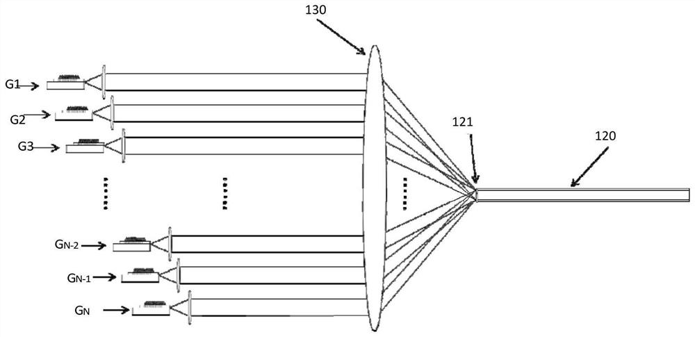
[0020] An embodiment of the present invention provides a semi-coherent beam combining system for semiconductor lasers, refer to figure 1 ,include:
[0021] The first semiconductor laser chip G 1 To the Nth semiconductor laser chip G n , the kth semiconductor laser chip G k The k-th laser is emitted, and the first laser to the N-th laser are space-combined to form a space-combined laser, N is an integer greater than or equal to 2, and k is greater than or equal to 1 and less than or equal to N;
[0022] An optical fiber 120, the incident end of the optical fiber 120 has a partially reflective film layer 121;
[0023] A focusing coupling mirror 130, the focusing coupling mirror 130 is adapted to couple the first laser to the Nth laser light in the spatially combined laser beams into the optical fiber 120, and the focusing coupling mirror 130 faces the incident end of the optical fiber 120 ;
[0024] The partially reflective film layer 121 reflects part of the kth laser ligh...
PUM
 Abstract
Description
Claims
Application Information