Semiconductor process equipment

A technology of process equipment and semiconductors, which is applied in semiconductor/solid-state device manufacturing, discharge tubes, electrical components, etc., and can solve problems such as difficult monitoring of the temperature of the dielectric window and inability to stably control the temperature of the dielectric window

Pending Publication Date: 2021-04-20
BEIJING NAURA MICROELECTRONICS EQUIP CO LTD
View PDF0 Cites 2 Cited by
  • Summary
  • Abstract
  • Description
  • Claims
  • Application Information

AI Technical Summary

Problems solved by technology

Existing semiconductor etching equipment is difficult to accurately monitor the temperature of the dielectric window, and cannot stably control the temperature of the dielectric window

Method used


Image

  • Semiconductor process equipment
  • Semiconductor process equipment
  • Semiconductor process equipment

Examples


Embodiment Construction

[0032] Specific embodiments of the present invention will be described in detail below in conjunction with the accompanying drawings. It should be understood that the specific embodiments described here are only used to illustrate and explain the present invention, and are not intended to limit the present invention.

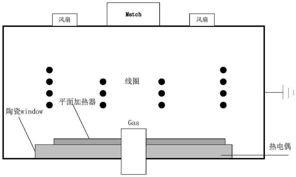
[0033] Such as figure 1 Shown is a structural schematic diagram of a dielectric window temperature control scheme in the prior art. A thermocouple is inserted on the side wall of the dielectric window, and the thermocouple is set close to the bottom surface of the dielectric window to detect the bottom surface of the dielectric window (that is, towards the process surface). In order to avoid affecting the electromagnetic field fed into the process chamber by the coil, the end of the thermocouple extending into the dielectric window does not exceed the range covered by the induction coil. However, the heating of the dielectric window by the heater is not uniform...


PUM


Abstract

The invention provides semiconductor process equipment. The equipment comprises a process chamber with a process window at the top, a control device, an edge temperature measuring piece, a first temperature measuring piece and a second temperature measuring piece, and the edge temperature measuring piece is inserted into the process window from the side wall of the edge of the process window and is arranged close to the bottom surface of the process window; the process window comprises a central area and an edge area surrounding the central area, the first temperature measuring piece and the second temperature measuring piece are both arranged above the process window, the first temperature measuring piece corresponds to the central area in position, and the second temperature measuring piece corresponds to the edge temperature measuring piece in position; and the control device is used for determining the temperature of the bottom surface of the central area of the process window according to the temperature detection values of the edge temperature measurement part, the first temperature measurement part and the second temperature measurement part. According to the invention, the control device can obtain the actual temperature of the bottom surface of the central area of the process window according to the temperature difference between the top surface and the bottom surface of the process window and the temperature of the top surface of the central area of the process window, thereby achieving the precise monitoring and control of the temperature of the bottom surface of the central area of the process window.

Description

technical field [0001] The present invention relates to the field of semiconductor process equipment, in particular to semiconductor process equipment. Background technique [0002] Semiconductor etching equipment usually includes a radio frequency power supply and a process chamber. The radio frequency energy provided by the radio frequency power supply is transmitted into the process chamber and ionizes special gases (such as argon Ar, helium He, nitrogen, etc.) under high vacuum in the process chamber. N 2 etc.) to generate plasma, complex interactions occur between these active particles and the wafer placed in the cavity and exposed to the plasma environment, so that various physical and chemical reactions occur on the surface of the wafer material, so that the surface properties of the material changes to complete the etching process of the wafer. [0003] During the semiconductor etching process, how to ensure the consistency of the temperature of the dielectric win...

Claims


Application Information

Patent Timeline
Patent Type & Authority Applications(China)
IPC IPC(8): H01L21/67H01J37/305
Inventor 程旭文
Owner BEIJING NAURA MICROELECTRONICS EQUIP CO LTD
Why Eureka
Try Eureka