

Pixel structure based on oxide thin film transistor, detector and production method thereof
A technology of oxide film and pixel structure, which is applied in the field of X-ray sensors, can solve problems such as performance degradation, achieve low leakage current, reduce electrical influence, and improve the effect of influence
- Summary
- Abstract
- Description
- Claims
- Application Information
AI Technical Summary
Problems solved by technology
Method used
Image

Examples
Embodiment 1
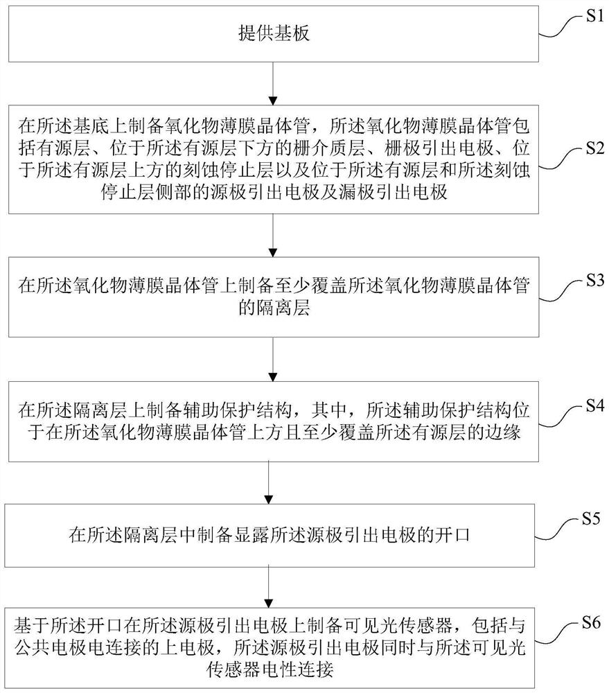
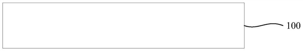
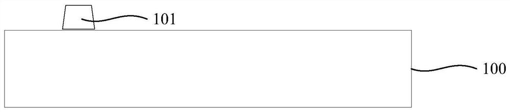
[0061] Such as Figure 15-17 shown, see Figure 1-15 , in order to achieve the above purpose and other related purposes, the present invention provides a pixel structure based on an oxide thin film transistor, and a new type of pixel structure based on an oxide thin film transistor can be effectively protected by introducing an auxiliary protection structure. The device is beneficial to reduce the leakage current of degraded thin film transistors such as photoelectric sensor film formation and high temperature process, thereby reducing the impact of subsequent manufacturing processes on the electrical properties of thin film transistors, and can effectively improve the hydrogen atoms in the preparation of visible light sensors. Impact, improve the process compatibility of oxide thin film transistors and photosensors, realize low leakage current of oxide thin film transistors and device electrical uniformity, thereby expanding the process window of the panel and improving the r...
Embodiment 2
[0111] Such as Figure 18 As shown, the present invention also provides an X-ray detector, including the pixel structure described in any one of the solutions in Embodiment 1, such as Figure 18 The pixel structure 202 in , wherein the pixel structure 202 constitutes the sensor array 201 of the X-ray detector, that is, a plurality of pixel units arranged two-dimensionally on the substrate constitutes the sensor array. In addition, the X-ray detector further includes at least a scintillator layer 203 and an encapsulation film layer 204 disposed above the sensor array 201 , and of course, may also include a lower encapsulation film layer 205 formed below the sensor array 201 .
[0112] Wherein, the packaging film layer 204 can be a reflective film / light-absorbing film / protective packaging film; the lower packaging film layer 205 can be a reflective film / light-absorbing film / protective packaging film; the detector substrate 200 on the lower surface of the sensor array 201 is the ...
PUM
| Property | Measurement | Unit |
|---|---|---|
| Thickness | aaaaa | aaaaa |
| Thickness | aaaaa | aaaaa |
| Thickness | aaaaa | aaaaa |
Abstract
Description
Claims
Application Information