Laser cutting and ring removing method for wafer

A laser cutting and wafer technology, applied in laser welding equipment, circuits, manufacturing tools, etc., can solve the problems of splashing ablation, micro-cracks in the effective area, etc.

Pending Publication Date: 2021-04-27
HUA HONG SEMICON WUXI LTD
View PDF10 Cites 0 Cited by
  • Summary
  • Abstract
  • Description
  • Claims
  • Application Information

AI Technical Summary

Problems solved by technology

[0011] However, as the thinner sheet technology develops, it will cause microcracks in the effective area during the Ring Remove process; if a wider laser beam is simply selected, the thermal effect per unit time w

Method used


Image

  • Laser cutting and ring removing method for wafer
  • Laser cutting and ring removing method for wafer
  • Laser cutting and ring removing method for wafer

Examples


Embodiment Construction

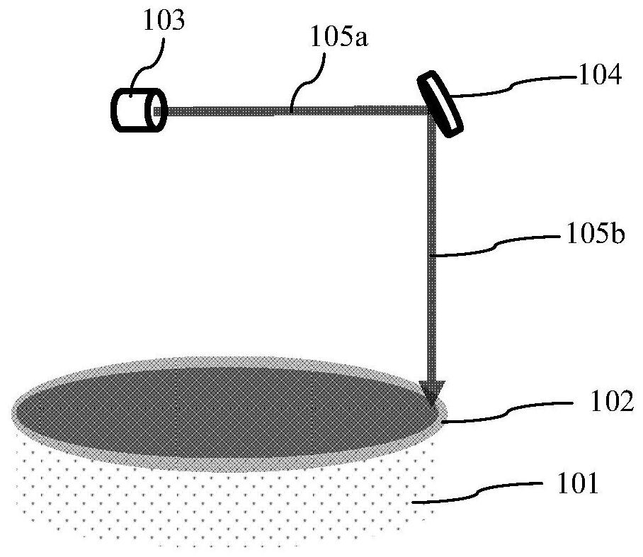
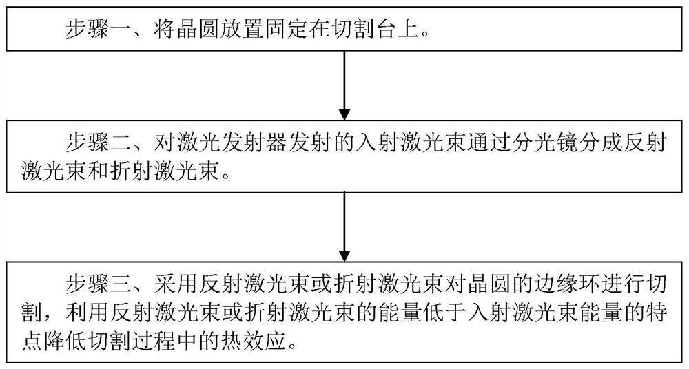
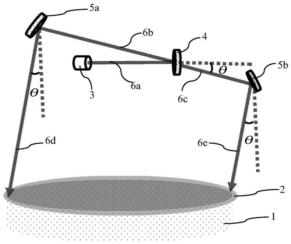
[0037] Such as figure 2 Shown is the flow chart of the laser cutting ring removal method of wafer 2 in the embodiment of the present invention; as image 3 As shown, it is a schematic diagram of laser dicing in the laser dicing and ring removal method of wafer 2 in the embodiment of the present invention. The laser cutting and deringing method of wafer 2 in the embodiment of the present invention comprises the following steps:

[0038] Step 1, placing and fixing the wafer 2 on the cutting table 1 .

[0039] The wafer 2 has been thinned.

[0040] The thinning process of the wafer 2 includes Taiko thinning.

[0041] The thinned wafer 2 has a thickness ranging from tens of microns to hundreds of microns.

[0042] The width of the edge ring to be cut on the wafer 2 is less than several millimeters.

[0043] Step 2: The incident laser beam 6a emitted by the laser emitter 3 is divided into a reflected laser beam 6b and a refracted laser beam 6c by a beam splitter 4, and the en...


PUM

PropertyMeasurementUnit
Angleaaaaaaaaaa

Abstract

The invention discloses a laser cutting and ring removing method for a wafer. The laser cutting and ring removing method comprises the following steps that 1, the wafer is placed and fixed to a cutting table; 2, an incident laser beam emitted by a laser emitter is divided into a reflected laser beam and a refracted laser beam through a spectroscope; and 3, the edge ring of the wafer is cut and removed by adopting the reflected laser beam or the refracted laser beam, and the heat effect in the cutting process is reduced by utilizing the characteristic that the energy of the reflected laser beam or the refracted laser beam is lower than that of the incident laser beam. According to the laser cutting and ring removing method, the width of the laser cutting light beam can be increased, the laser cutting light beam is ensured to have lower energy so that the heat effect in the cutting process can be reduced, ablative substances are prevented from splashing to the surface of the wafer on the inner side of the edge ring, adverse effects on effective chip crystal grains of the wafer can be prevented, and meanwhile, the wider laser cutting light beam is beneficial to cutting of the thinner wafer without generating micro cracks.

Description

technical field [0001] The invention relates to a semiconductor integrated circuit manufacturing process method, in particular to a laser cutting ring cutting method for a wafer. Background technique [0002] In the manufacture of semiconductor integrated circuits, the wafer often needs to be thinned to improve the performance of the device. After the wafer is thinned, the edge ring of the wafer needs to be cut and removed. The wafer thinning process includes a Taiko thinning process. The Taiko thinning only thins the middle area of ​​the wafer, and the edge area of ​​the wafer is not thinned but serves as a support ring. [0003] Cutting processes for edge rings of wafers include laser cutting, such as figure 1 As shown, it is a schematic diagram of laser cutting in the laser cutting and ring removal method of the existing wafer; the laser cutting and ring removal method of the existing wafer includes the following steps: [0004] Step 1, placing and fixing the wafer 102 ...

Claims


Application Information

Patent Timeline
IPC IPC(8): B23K26/38B23K26/067B23K26/064
CPCB23K26/38B23K26/067B23K26/064B23K26/0643B23K2101/40
Inventor 惠科石苏亚青谭秀文
Owner HUA HONG SEMICON WUXI LTD
Why Eureka
Try Eureka